Method for manufacturing gallium nitride nano-wire with tungsten auxiliary heat anneal

A technology of nanowires and auxiliary heat, applied in gaseous chemical plating, semiconductor/solid-state device manufacturing, ion implantation plating, etc., can solve the problems of high requirements for gas path structure and experimental equipment, and achieve the effect of low preparation requirements

Inactive Publication Date: 2010-06-09
DAHOM FUJIAN ILLUMINATION TECH
View PDF2 Cites 0 Cited by
  • Summary
  • Abstract
  • Description
  • Claims
  • Application Information

AI Technical Summary

Problems solved by technology

[0006] However, the above preparation methods have relatively high requirements on the reaction source, gas path structure and experimental equipment.

Method used


Image

  • Method for manufacturing gallium nitride nano-wire with tungsten auxiliary heat anneal
  • Method for manufacturing gallium nitride nano-wire with tungsten auxiliary heat anneal
  • Method for manufacturing gallium nitride nano-wire with tungsten auxiliary heat anneal

Examples


Embodiment 1

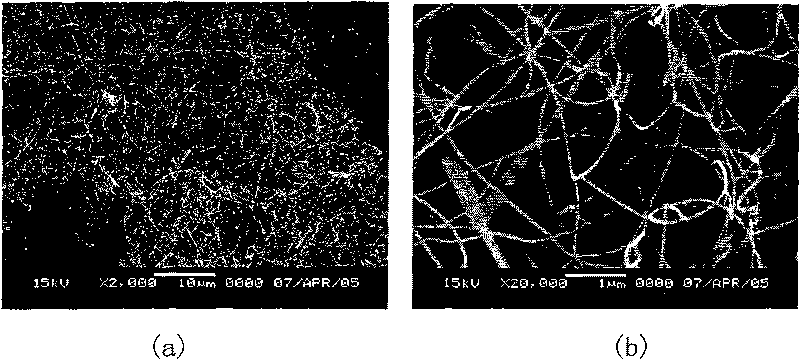
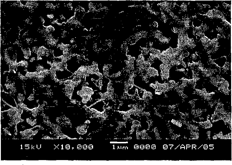
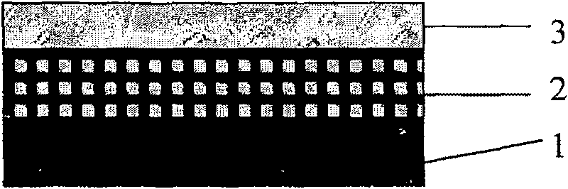
[0022] Embodiment 1: adopt MOCVD method in Al 2 o 3 A GaN film with a thickness of 2 microns was epitaxially grown on the substrate, and this film was used as a template, and an 8nm thick metal W thin layer was deposited on the template at a temperature of 500°C by electron beam evaporation, and then the metal layer with the metal layer The template is put into the thermal annealing reaction chamber, under N 2 The atmosphere was heated up to 1050°C and annealed for 20 minutes. The sample measurement results show that the GaN nanowires grown by this method have a diameter between 10 and 100 nm and a high aspect ratio.

Embodiment 2

[0023] Embodiment 2: The same result can be obtained by using the method as in Embodiment 1 with SiC, Si or GaAs as the substrate.


PUM

PropertyMeasurementUnit
thicknessaaaaaaaaaa
diameteraaaaaaaaaa
lengthaaaaaaaaaa

Abstract

The invention which relates to a method for preparing GaN nanometer lines by assisting the thermal annealing with tungsten is characterized by adopting the metallic tungsten (W) as a catalyst; in theprocess of preparing the GaN nanometer lines with the thermal annealing, a GaN nanometer line is formed through thermal annealing in the atmosphere of N2 after a thin W layer is evaporated from electron beams of a GaN template. The metallic tungsten thin film is introduced as the catalyst for the growth GaN nanometer lines, and the metallic W can aggregate at high temperature while the GaN at a lower layer is decomposed to cause the metallic W layer to form separate porous netted structure so as to expose partial GaN films, and at the same time, the separated metallic Ga and N atoms are combined into slender GaN nanometer lines under the effect of the catalyst of metallic W. The method is simple and easily implemented only by depositing or sputtering a thin metallic W layer and is suitablefor scientific experiments and batching production.

Description

technical field [0001] The invention relates to a preparation method for preparing gallium nitride (GaN) nanowires by tungsten-assisted thermal annealing. The invention aims at making high-quality, high-aspect-ratio GaN nanowires, and belongs to the technical field of material preparation. Background technique [0002] Low-dimensional structure semiconductor materials exhibit many excellent properties due to quantum effects, which has aroused great enthusiasm for research. Due to the confinement effect of the quantum size, the electronic energy state of the quantum wire material presents a V-shaped, T-shaped or oblique T-shaped energy level structure similar to atom splitting. Due to the separation of energy levels, quantum wire materials are more likely to meet the requirements of particle number inversion necessary for lasers, so they are suitable for making lasers. At the same time, quantum wires are used to make lasers. Due to the quantum confinement effect, the thres...

Claims


Application Information

Patent Timeline
Patent Type & Authority Patents(China)
IPC IPC(8): C23C16/34C23C14/32C23C14/34H01L21/20H01L21/205
Inventor 林朝通于广辉雷本亮王新中王笑龙齐鸣
Owner DAHOM FUJIAN ILLUMINATION TECH
Why Eureka
Try Eureka