Method for preparing dielectric film embedded with high-density palladium nano-crystal

A dielectric thin film, palladium nanotechnology, applied in the field of semiconductor memory manufacturing, can solve the problems of difficult control of nanocrystal size and distribution, limited surface density of nanocrystals, etc., achieve good charge storage effect, low rapid thermal annealing temperature, reduce Effects of thermal damage and energy consumption

Inactive Publication Date: 2010-11-24
FUDAN UNIV
View PDF4 Cites 0 Cited by
  • Summary
  • Abstract
  • Description
  • Claims
  • Application Information

AI Technical Summary

Problems solved by technology

The currently reported nanocrystals are mainly grown in two-dimensional distribution. [5] , since the size and distribution of nanocrystals are not easy to control, the areal density of nanocrystals is relatively limited

Method used


Image

  • Method for preparing dielectric film embedded with high-density palladium nano-crystal
  • Method for preparing dielectric film embedded with high-density palladium nano-crystal
  • Method for preparing dielectric film embedded with high-density palladium nano-crystal

Examples


Embodiment

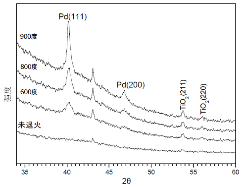
[0023] After standard cleaning of P-type (100) silicon wafers, a layer of Al with a thickness of about 6nm was grown by atomic layer deposition (ALD) 2 o 3 thin film, as a charge tunneling layer. Put the silicon wafer covered with the above film into the magnetron sputtering reaction chamber, and the two targets for co-sputtering are Pd and Ti. The sputtering condition is: chamber vacuum degree 4.2×10 -5 Pa, argon (Ar) flow rate is 37sccm, oxygen (O 2 ) flow rate is 4 sccm, the DC power applied to the Pd target and Ti target is 25W and 100W respectively, the working pressure is 0.72Pa, the substrate is not heated, the substrate rotation speed is 8 rpm, and the total sputtering time is 840 seconds. Test analysis shows that the film obtained by co-sputtering method is palladium oxide (PdO x ) and titanium oxide (TiO x ) of the mixed film. Next, put the obtained sample into a rapid thermal annealing furnace for rapid thermal annealing, and the annealing atmosphere is nitrog...


PUM

PropertyMeasurementUnit
particle diameteraaaaaaaaaa
particle sizeaaaaaaaaaa
thicknessaaaaaaaaaa

Abstract

The invention belongs to the technical field of semiconductor memory manufacturing and in particular relates to a method for preparing a dielectric film embedded with a high-density palladium nano-crystal. The method comprises the steps of performing co-sputtering in oxygen atmosphere to deposit the dielectric film which contains palladium oxide and performing high-temperature fast thermal annealing treatment to obtain the dielectric film embedded with the high-density palladium nano-crystal, wherein the diameter of the palladium nano-crystal is about 3 to 15 nanometers. The dielectric film embedded with the high-density palladium nano-crystal prepared by the method shows good charge storage effect when used as a charge trapping layer in a flash device.

Description

technical field [0001] The invention belongs to the technical field of manufacturing semiconductor memory, and in particular relates to a method for preparing an embedded high-density palladium nanocrystal dielectric thin film, which can be used for a charge trapping layer in a flash memory device. technical background [0002] With the continuous development of semiconductor process technology, the flash memory market has developed rapidly in the past few decades. According to the 2007 ITRS forecast, by 2020, the size of flash memory cells will be reduced to 1000nm 2 . The traditional non-volatile flash memory based on polysilicon floating gate faces a series of problems after the 65nm technology node, the most important one is the degradation of data retention ability caused by the thinning of the tunnel oxide layer [1] . Compared with the traditional floating gate structure, the use of discrete charge storage technology can improve the data retention time of the memory ...

Claims


Application Information

Patent Timeline
Patent Type & Authority Applications(China)
IPC IPC(8): H01L21/285H01L21/8247C23C14/35
Inventor 丁士进黄万一
Owner FUDAN UNIV
Why Eureka
Try Eureka