Pixel structure and its production method

A pixel structure and conductive pattern technology, which is applied in semiconductor/solid-state device manufacturing, optics, instruments, etc., can solve the problems of increasing parasitic capacitance, affecting the pixel aperture ratio, and increasing the size, so as to achieve high aperture ratio and reduce crosstalk effect Effect

Active Publication Date: 2008-07-16
AU OPTRONICS CORP
View PDF0 Cites 12 Cited by
  • Summary
  • Abstract
  • Description
  • Claims
  • Application Information

AI Technical Summary

Problems solved by technology

However, when the transparent pixel electrode is too close to the data line, the parasitic capacitance (Cpd, capacitance between pixel and data line) it receives will become larger, causing the fully charged charge on the pixel electrode to be lost in the next frame. ) before the conversion, there will be a crosstalk effect (cross talk) due to the different voltages transmitted by the data lines
In addition, when the distance between the common electrode and the data line is too close, the parasitic capacitance it receives will increase, and crosstalk effect will also occur.
[0003] In order to reduce the effect of parasitic capacitance, many methods have been studied, such as increasing the size of the storage capacitor, which can reduce the ratio of parasitic capacitance to all capacitance affecting a sub-pixel unit (sub-pixel). However, if the area is increased Increasing the storage capacitance will affect the pixel aperture ratio

Method used


Image

  • Pixel structure and its production method
  • Pixel structure and its production method
  • Pixel structure and its production method

Examples


Embodiment Construction

[0042] In order to enable examiners and those familiar with the art to further understand the present invention, the preferred embodiments of the present invention are listed below, together with the accompanying drawings, component symbols, etc., to describe in detail the composition of the present invention and the desired effects .

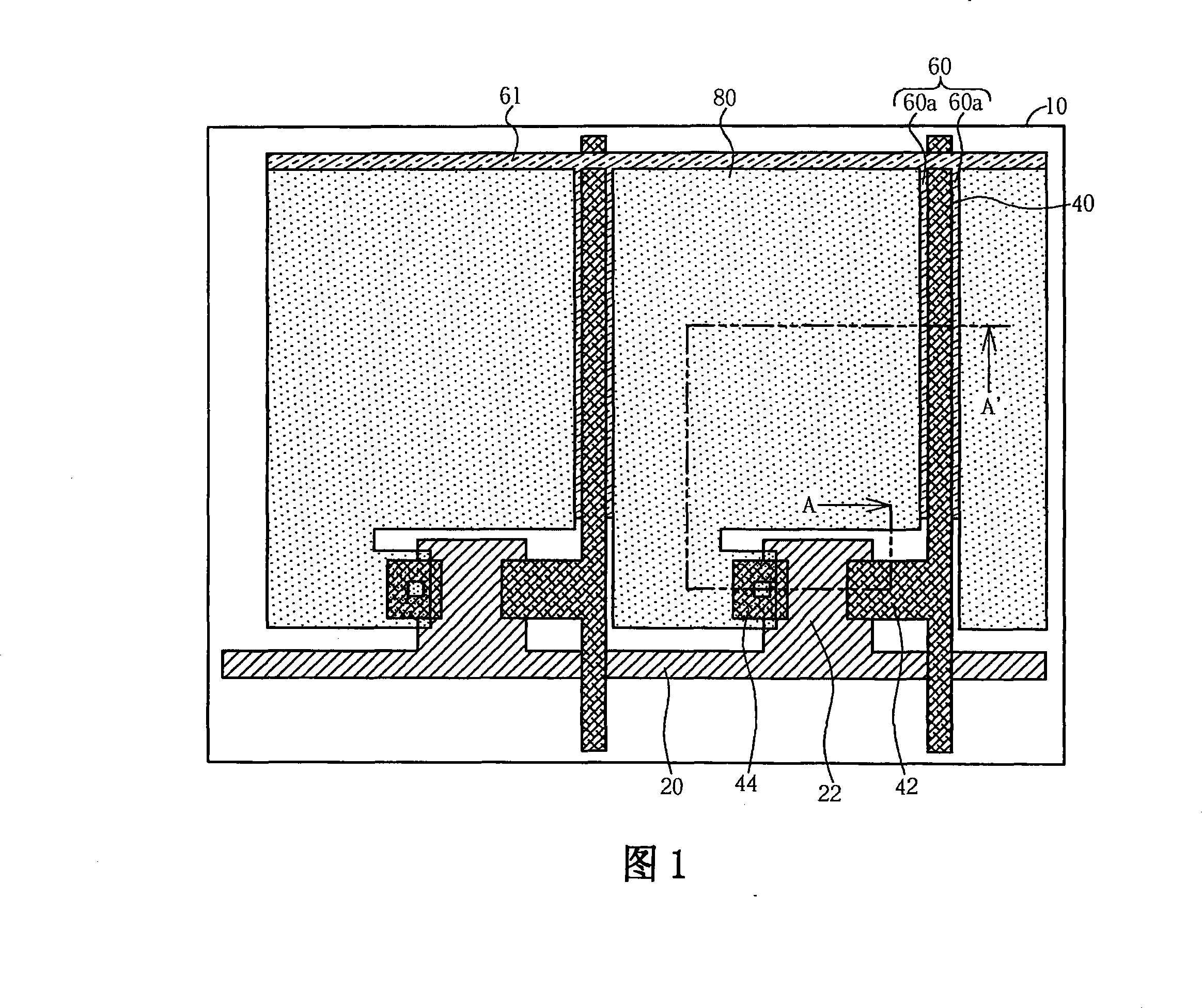
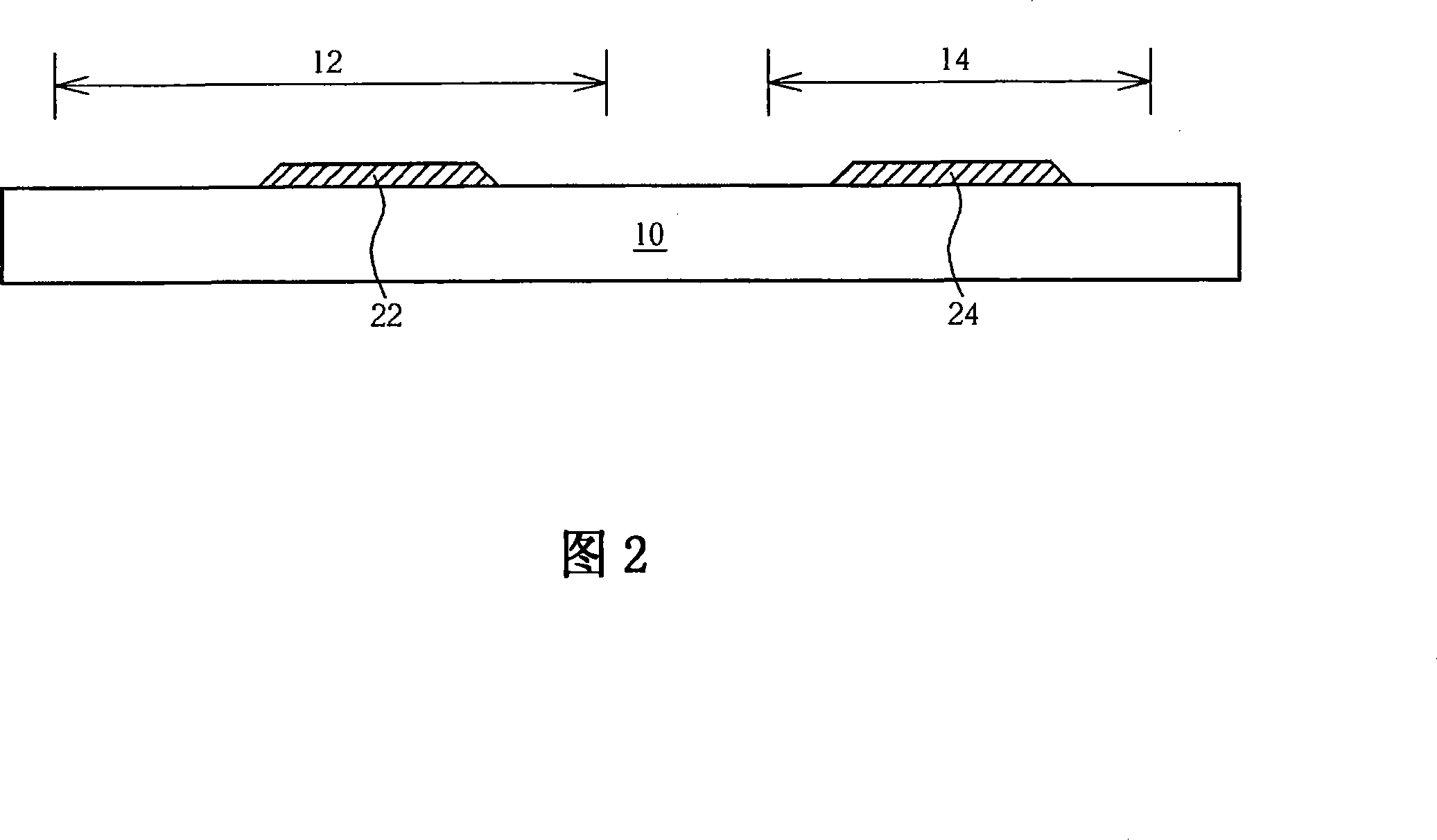
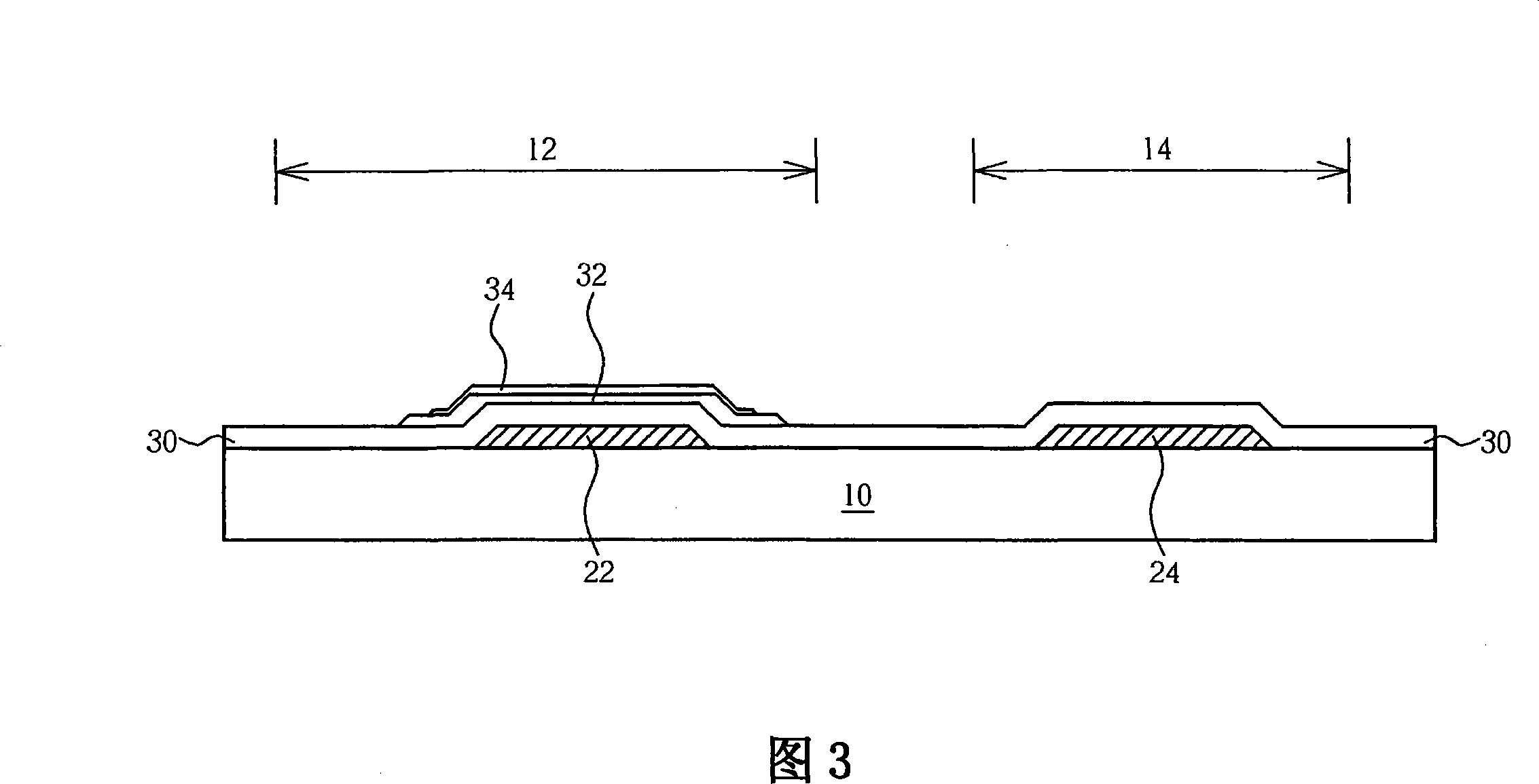
[0043] This embodiment illustrates the present invention by taking the pixel structure of an amorphous silicon thin film transistor liquid crystal display device as an example, but the application of the pixel structure of the present invention is not limited thereto, and can be applied to the pixel structure of other types of liquid crystal display devices. Please refer to Figures 1 to 7. Figure 1 is a schematic diagram of a pixel structure in a preferred embodiment of the present invention, and Figures 2 to 7 are schematic cross-sectional views of manufacturing the pixel structure in Figure 1, wherein Figure 1 shows a schematic top view of th...


PUM


Abstract

The invention provides a pixel structure and the production method thereof. The pixel structure comprises a substrate, a shading pattern floatingly arranged on the substrate, an insulation layer arranged on the substrate and the shading pattern, a data line arranged above the shading pattern and corresponding to the shading pattern, a dielectric layer arranged on the data line and the insulation layer, and a third-layer conductive pattern arranged on the dielectric layer. The third-layer conductive pattern comprises a common wire and a common pattern, wherein, the common pattern has two branch lines, a gap exists between the two branch lines, and further more the gap is positioned above the data line. The pixel structure of the invention takes advantage of the shading pattern of a first-layer conductive pattern to shield the light leakage which is easy to be produced on both sides of the data line of a second-layer conductive pattern, and takes advantage of the common pattern of the third-layer conductive pattern to shield the pixel electrode and the data line to avoid the parasitic capacitance produced between the pixel electrode and the data line.

Description

technical field [0001] The present invention relates to a pixel structure and a manufacturing method thereof, in particular to a pixel structure with an ultra-high aperture ratio and a manufacturing method thereof. Background technique [0002] In the manufacture of liquid crystal displays, the size of the pixel aperture ratio directly affects the utilization rate of the backlight source, and also affects the display brightness of the panel. The main factor affecting the aperture ratio is the distance between the transparent pixel electrode and the data line. To pursue a larger aperture ratio, the distance between the transparent pixel electrode and the data line must be shortened during layout. However, when the transparent pixel electrode is too close to the data line, the parasitic capacitance (Cpd, capacitance between pixel and data line) it receives will become larger, causing the fully charged charge on the pixel electrode to be lost in the next frame. ) before conver...

Claims


Application Information

Patent Timeline
Patent Type & Authority Applications(China)
IPC IPC(8): H01L27/12H01L23/522H01L21/84H01L21/768G02F1/1362
Inventor 陈茂松石志鸿江怡禛
Owner AU OPTRONICS CORP
Why Eureka
Try Eureka