
Semiconductor light emitting device and method for manufacturing the same

A technology for light-emitting devices and manufacturing methods, applied in semiconductor devices, electrical components, circuits, etc., can solve the problems of poor chip current expansion, reduced light extraction efficiency, poor heat dissipation performance, etc., to improve current expansion effect and improve heat transfer performance. , the effect of eliminating the current blocking effect

Inactive Publication Date: 2011-05-04
SUN YAT SEN UNIV
View PDF1 Cites 0 Cited by
  • Summary
  • Abstract
  • Description
  • Claims
  • Application Information

AI Technical Summary

Problems solved by technology

However, in order to reduce the voltage, the high-resistance buffer layer needs to be removed before making the N-electrode, which is easy to damage the chip and increase the process cost, and the N-electrode covered on the N-type layer will block part of the light, reducing the light extraction efficiency
Solving the problems of poor current expansion and poor heat dissipation of GaN-based LED chips on sapphire substrates is of great significance for the wide application of GaN-based LEDs on sapphire substrates

Method used


Image

  • Semiconductor light emitting device and method for manufacturing the same
  • Semiconductor light emitting device and method for manufacturing the same
  • Semiconductor light emitting device and method for manufacturing the same

Examples


Embodiment 1

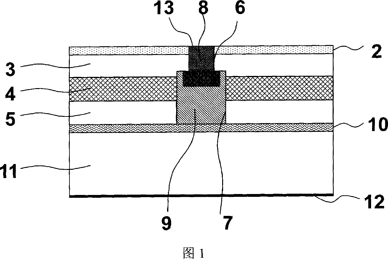
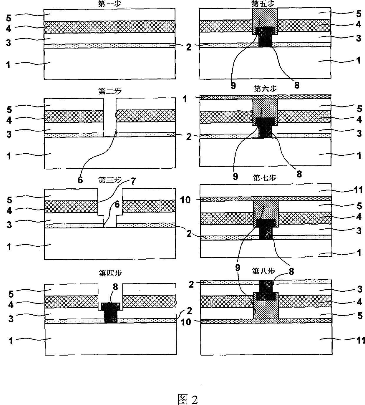
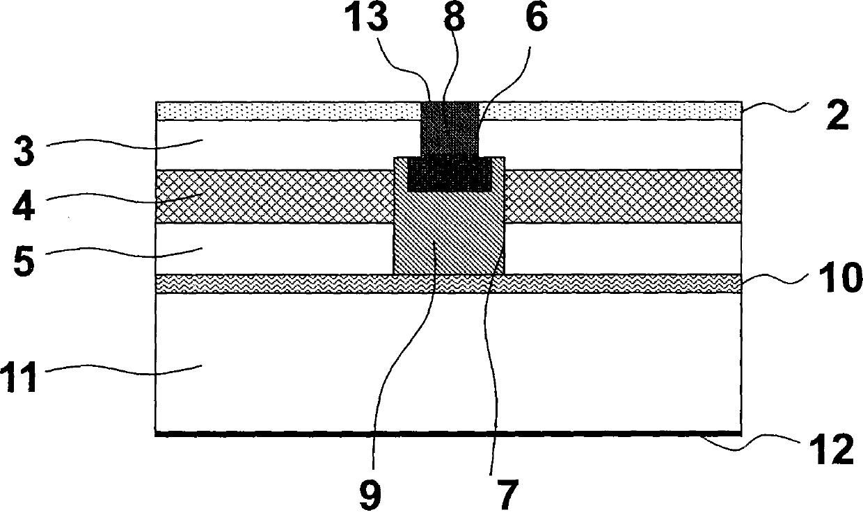
[0028] Referring to FIG. 1, a semiconductor light-emitting device includes a conductive substitute substrate 11 and a semiconductor epitaxial stack connected to the substrate 11 through a metal layer 10. The semiconductor epitaxial stack includes a buffer layer 2, N-type layer 3 , light-emitting layer 4 and P-type layer 5 . The N-type layer 3 is provided with a conductor, one end of which extends upward to expose the buffer layer 2, and is provided with an N-type electrode 13, and an insulating medium layer is arranged between the other end and the metal layer 10, and the lower end of the substitute substrate is a P electrode 12 .

[0029] The conductor is composed of a columnar small through hole 6 and a conductive substance 8 filled in the small through hole 6. The conductor is only in contact with the buffer layer 2, the sidewall of the N-type layer 3 and the lower edge of the N-type layer 3, It is not in contact with the light-emitting layer 4, the P-type layer 5 and the ...


PUM


Abstract

The invention discloses a semiconductor light-emitting device, which comprises a substitution substrate and a semiconductor extension laminated layer which is orderly connected with the substitution substrate through a metal layer, wherein the semiconductor extension laminated layer at least comprises a buffer layer, an N type layer, a luminous layer and a P type layer from the upper to the lower, a conductor is arranged in the N type layer, one end of the N type layer extents to expose the buffer layer, and an N type electrode is arranged, and a dielectric layer is arranged between the otherend of the conductor and the metal layer. The lower end of the substitution substrate is quipped with a P type electrode, and the conductor, the P type layer and the metal layer are separated. The device of the invention sends light from the side of the N type layer, a transparency electrode does not need to use on the side of sending the light, thereby being capable of effectively improving the output power of the semiconductor device, and also being capable of reducing the thermal resistance of a light emitting diode device. Further, the invention also discloses a method for preparing a semiconductor light emitting diode.

Description

technical field [0001] The present invention relates to a semiconductor light-emitting device and a manufacturing method thereof. Background technique [0002] III-V nitride semiconductor materials are widely used in violet, blue, green and white light-emitting diodes, violet lasers for high-density optical storage, ultraviolet light detectors, and high-power high-frequency electronic devices. However, due to the lack of suitable substrates, high-quality GaN-based material films are usually grown on sapphire or SiC substrates, but SiC substrates are expensive and small in size. GaN-based material films are most commonly grown on sapphire substrates and have the most mature applications, but sapphire substrates have disadvantages such as high hardness, non-electrical conductivity, and poor thermal conductivity. [0003] Due to the insulating properties of the sapphire substrate, the P and N electrodes of the light-emitting diode chip are in the form of coplanar electrodes, t...

Claims


Application Information

Patent Timeline
Patent Type & Authority Patents(China)
IPC IPC(8): H01L33/00H01L33/14H01L33/38H01L33/64
Inventor 张佰君王钢范冰丰
Owner SUN YAT SEN UNIV
Learn More