Booster circuit

A technology of booster circuit and comparison circuit, which is applied in the direction of conversion equipment without intermediate conversion to AC, can solve the problems of increasing current consumption, decreasing boosting efficiency, and increasing layout area, so as to suppress current consumption and improve boosting. Efficiency, the effect of suppressing the increase of the layout area

Inactive Publication Date: 2008-07-23
PANASONIC CORP
View PDF3 Cites 3 Cited by
  • Summary
  • Abstract
  • Description
  • Claims
  • Application Information

AI Technical Summary

Problems solved by technology

[0010] However, since the above-mentioned conventional boost circuit 901 connects the source of the charge transfer transistor 906 to the N-well 908, the N-well 908 is charged with the voltage shift amplitude of the clock signals CLK1 and CLK2 according to the voltage shift of the clock signals CLK1 and CLK2. The formed parasitic capacitance is charged and discharged, and as a result, there is a problem that the current consumption increases
[0011] Furthermore, since the charge supplied by the clock signals CLK1 and CLK2 is used as charge and discharge charge of the N well 908, there is a problem that the boosting efficiency decreases.
[0012] In addition, since the source of the charge transfer transistor 906 is connected to the N well 908, the N well 908 needs to be separated between the charge transfer transistors 906, and thus, there is a problem that the layout area increases.

Method used


Image

  • Booster circuit
  • Booster circuit
  • Booster circuit

Examples


Embodiment Construction

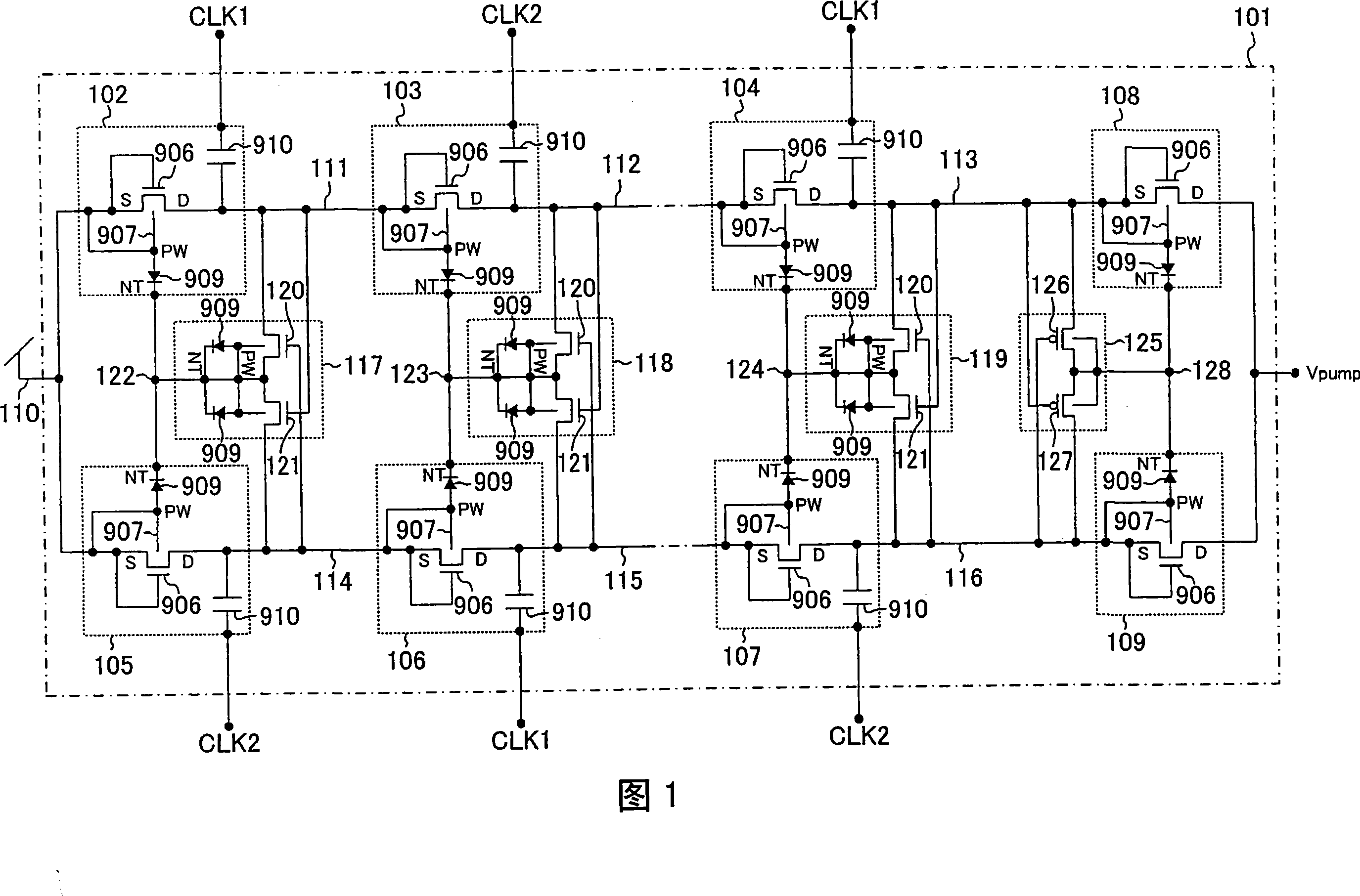
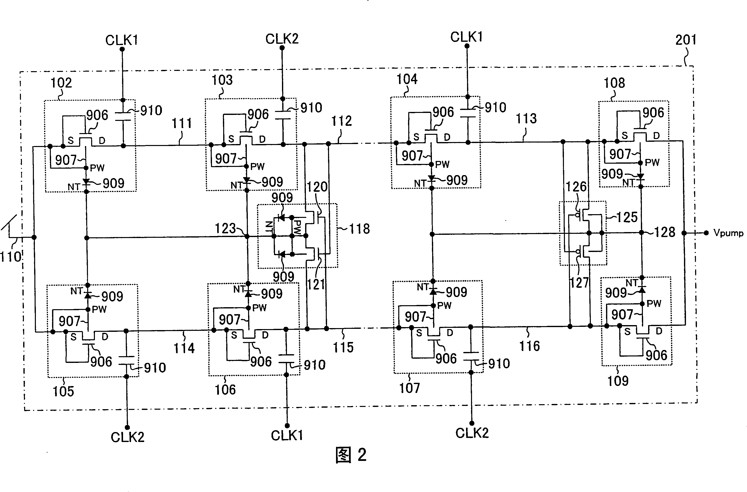
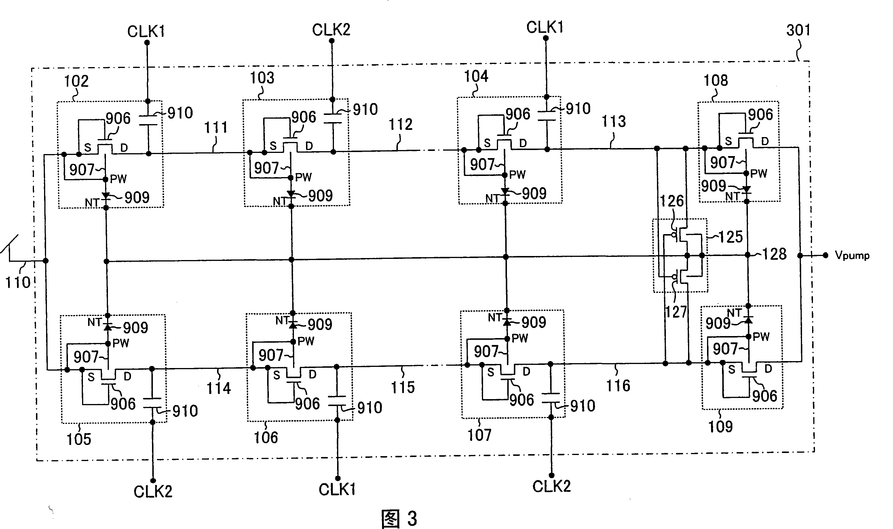
[0092] Hereinafter, a booster circuit according to an embodiment of the present invention will be described with reference to the drawings.

[0093] FIG. 1 shows a configuration example of a booster circuit according to the present invention. In FIG. 1 , 101 is a dual-parallel booster circuit that generates an output terminal voltage (boosted voltage) Vpump by inputting two-phase clock signals CLK1 and CLK2 to perform a boosting operation. 102, 103, 104, 105, 106, and 107 have the structure of the first column and the second column, and input CLK1 to the odd-numbered stage in the first column, input CLK2 to the even-numbered stage in the first column, and input CLK2 to the odd-numbered stage in the second column Input CLK2, input CLK1 boost unit to the even-numbered stage of the second column; 108, 109 are anti-reverse current circuits for preventing reverse current of the boost voltage Vpump, 110, 111, 112, 113, 114, 115, 116 117, 118, and 119 are the input and output termin...


PUM


Abstract

A boosting circuit comprises a first boosting cell row and a second boosting cell row. The boosting circuit further comprises an analog comparison circuit for comparing the potential of boosting cells on the same stage, and selecting and outputting the lower or higher of the potentials. The potential of an N well is controlled using the output potential of the analog comparison circuit. Thereby, the amplitude of an N well potential can be suppressed, and a single N well region can be shared. Thus, the boosting circuit can suppress reducing electric charge transmission efficiency, and realizing lower electric consumption and cutting down allocation area by controlling N well potential of the switching element having triple well structure.

Description

technical field [0001] The present invention relates to a voltage boosting circuit using a switching element of a triple well structure. Background technique [0002] In recent years, in flash memory (flash memory), which is a kind of nonvolatile semiconductor storage device, data reading and data rewriting under a single power supply voltage or a low power supply voltage are required, and when each operation is performed, a A boost circuit that provides a positive or negative boost voltage is required. Also, even in the CMOS process, the power supply voltage generated by the booster circuit is used to improve the characteristics of the analog circuit. [0003] Conventionally, a booster circuit using a switching element with a triple well structure is known (refer to the specifications of US Pat. Nos. 6,100,557, 6,121,821, and 7,102,422). [0004] Fig. 25 shows an example of a conventional booster circuit. In FIG. 25 , 901 is a booster circuit that receives two-phase cloc...

Claims


Application Information

Patent Timeline
Patent Type & Authority Applications(China)
IPC IPC(8): H02M3/07
Inventor 山平征二
Owner PANASONIC CORP
Why Eureka
Try Eureka