Passivation method for shunt bug of non-crystal silicon film light voltage module

A technology of amorphous silicon thin film and photovoltaic module, applied in photovoltaic power generation, climate change adaptation, sustainable building, etc., can solve the problems of slow laser scribing, high cost, poor stability of amorphous silicon alloy, etc., and achieve less shunt defects, The effect of high output power and high yield

Inactive Publication Date: 2008-08-06
BEIJING XINGZHE MULTIMEDIA TECH
View PDF10 Cites 4 Cited by
  • Summary
  • Abstract
  • Description
  • Claims
  • Application Information

AI Technical Summary

Problems solved by technology

This destructive method has the following disadvantages: laser scribing is slow and expensive; the format does not appear to be uniform; the transparency gradually increases with the reduction of the optoelectronic active area (loss of module function)
However, in practice, this method of overcoming shunting is not feasible for the following two reasons: First, because amorphous silicon alloys with wide band gaps such as amorphous silicon carbon are very poorly stable, it will degrade the efficiency of solar cells. Decays rapidly in light
The second is that the low electronic performance of the i-layer of the wide bandgap amorphous silicon alloy will seriously affect the output power of photovoltaic devices.
And doped amorphous silicon carbon or other alloys are not suitable for separate shunt suppression layer
Therefore, if figure 1 The shown method of adding a shunt suppression layer 70 on the standard i-layer 50 cannot effectively or permanently solve the shunt problem caused by the thin-film amorphous silicon i-layer 50

Method used


Image

  • Passivation method for shunt bug of non-crystal silicon film light voltage module
  • Passivation method for shunt bug of non-crystal silicon film light voltage module
  • Passivation method for shunt bug of non-crystal silicon film light voltage module

Examples


Embodiment 1

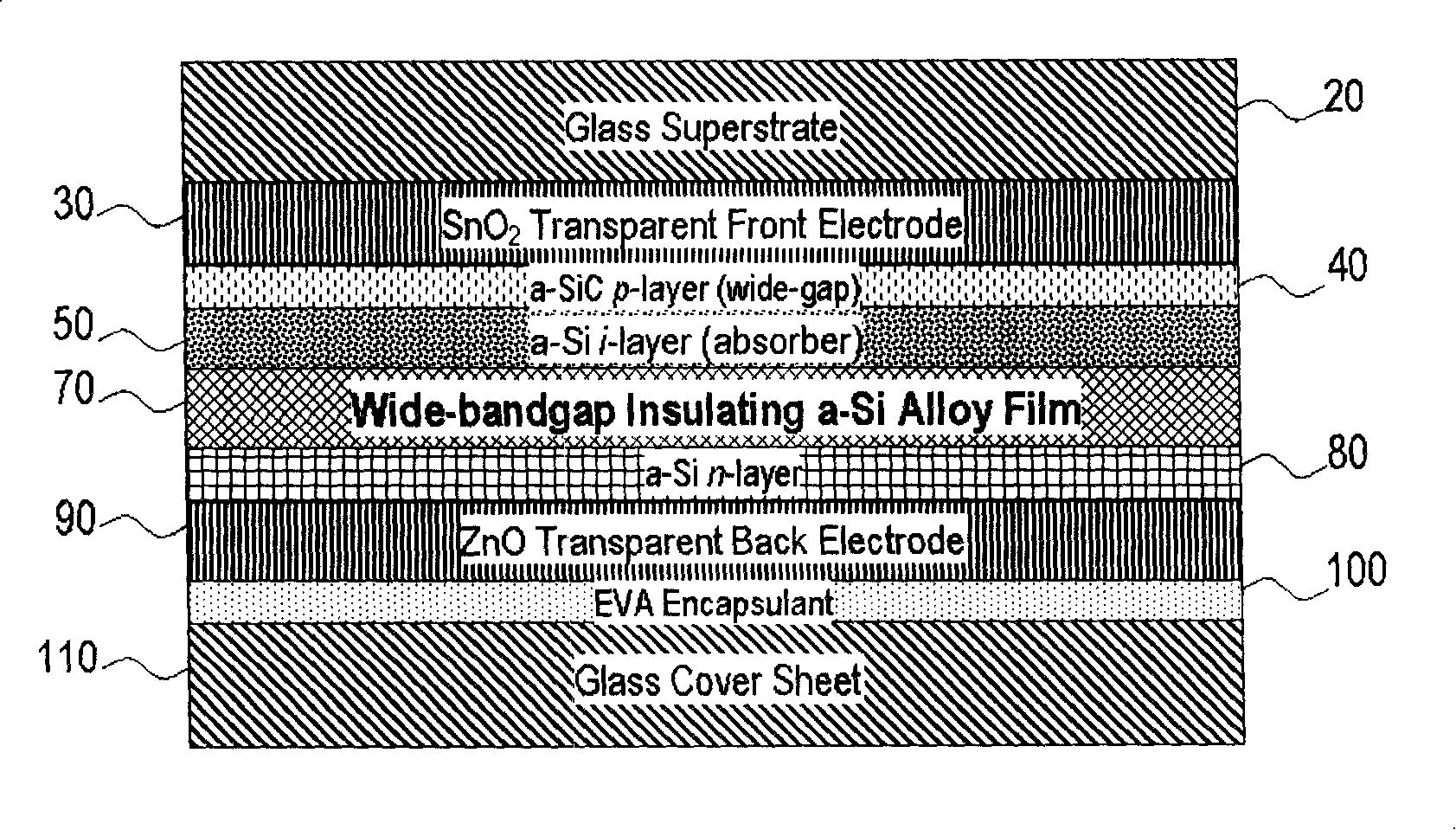
[0030] The invention relates to a simple, low-cost and high-efficiency method for eliminating shunt defects, which is suitable for a see-through photovoltaic module containing a relatively thin amorphous silicon active absorption conversion layer.

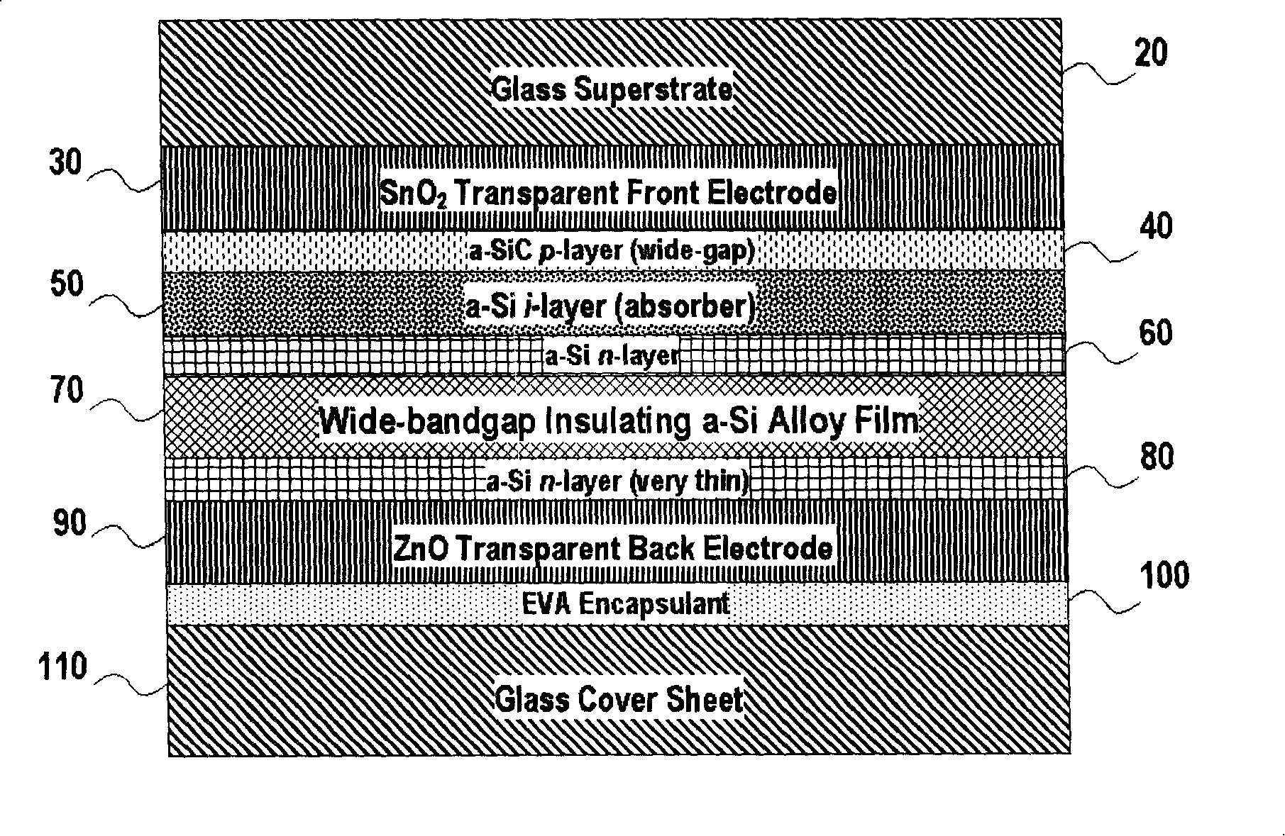
[0031] An implementation of the current invention, consisting of figure 2 explained. figure 2 is a cross-sectional view of a glass-encapsulated amorphous silicon solar cell based on figure 1 The p-i-n structure shown, but corrected. The only change in the device structure is that a first n-layer 60 based on amorphous silicon is added between the amorphous silicon i-layer and the wide-bandgap amorphous silicon-based shunt suppression layer 70 . In this p-i-n-"i"-n structure ( figure 2 40-50-60-70-80 in ), the shunt suppression "i" layer 70 and the second n-layer 80 form a double-layer suppression structure that acts as a shunt barrier, preventing any form of The diversion caused by the defect. The part that plays a role in t...

Embodiment 2

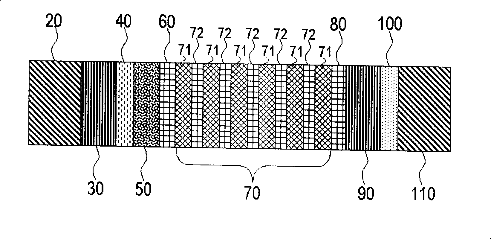
[0037] In fact, in order to make the building-integrated photovoltaic glass window more transparent, the amorphous silicon i-layer 50 needs to be made as thin as possible, but this will lead to more serious shunts. Therefore, the shunt suppression layer 70 based on amorphous silicon must be made as thick as possible to enhance its shunt prevention capability. However, for a given resistivity, if the shunt suppression layer "i" layer 70 is too thick, figure 2 A p-i-n-"i"-n-type device in will lose its energy conversion efficiency due to resistive losses in the "i" layer 70. To solve this problem, we can modify the shunt suppression structure of "i"-n (shunt suppression layer 70 and second n layer 80) by replacing a single thicker film layer with a series of thinner "i"-n bilayer films The shunt suppression layer 70. This concept is image 3 explained in. In this example, the shunt suppression layer 70, which plays the role of shunt passivation, is composed of many superimp...


PUM

PropertyMeasurementUnit
thicknessaaaaaaaaaa
thicknessaaaaaaaaaa
thicknessaaaaaaaaaa

Abstract

The present invention provides a method for restraining shunt defects of a p-i-n type large area photovoltaic module based on a hydrogenated amorphous silicon film, and the module comprises a comparatively thin i layer. An amorphous silicon alloy based film having wide band gap and high resistance is arranged between an active photovoltaic layer and a conductive back electrode to perform a barrier function upon the leakage of current. Shunt barrier material with strong light transmittance is a virtual film or is called a 'dead layer', which does not participate to photoelectrical power conversion directly. Shunt passivation films, like amorphous silicon devices which can be massively produced, are capable of realizing simple and quick production in plasma reinforcing chemical vapor deposition devices. The method especially contributes to enhancing the performance, product rate and reliability of perspective type or partial transparent film silicon photovoltaic modules applied to the application of building integrated photovoltaic.

Description

technical field [0001] The invention belongs to the field of photoelectric equipment, in particular to the technology of amorphous silicon thin-film solar cells. Background technique [0002] Photovoltaic (PV) systems are rapidly expanding their market in energy and industrial technology development due to the increasing demand for clean, safe, sustainable and reliable energy. Hydrogenated amorphous silicon (a-Si) thin films, and related amorphous silicon alloys with various light energy band gaps, are suitable for making various light-absorbing materials with different predetermined thicknesses, and have become a relatively mature material for commercial production of photovoltaic modules. branch. Thin-film silicon photoelectric technology has low material cost, large coverage area, and good benefits, especially it is easy to combine with building materials such as windows, roofs, and walls. Due to its relatively wide optical bandgap, amorphous silicon is particularly sui...

Claims


Application Information

Patent Timeline
Patent Type & Authority Applications(China)
IPC IPC(8): H01L31/075H01L31/042H01L31/0216
CPCY02B10/10Y02E10/50Y02A30/60Y02E10/548
Inventor 李沅民马昕
Owner BEIJING XINGZHE MULTIMEDIA TECH
Why Eureka
Try Eureka