Method and system for wafer inspection

A technology of wafers and inspectors, which is applied in the direction of originals for photomechanical processing, photolithography of patterned surfaces, image data processing, etc., can solve the problems of time-consuming, expensive masks, etc. when the effect

Active Publication Date: 2008-08-13
TAIWAN SEMICON MFG CO LTD
View PDF0 Cites 21 Cited by
  • Summary
  • Abstract
  • Description
  • Claims
  • Application Information

AI Technical Summary

Problems solved by technology

However, periodic inspection and re-qualifying of reticles is costly and time-consuming

Method used


Image

  • Method and system for wafer inspection
  • Method and system for wafer inspection
  • Method and system for wafer inspection

Examples


Embodiment Construction

[0062] In order to further explain the technical means and effects of the present invention to achieve the intended purpose of the invention, the specific implementation methods, methods and steps of the wafer inspection method and system proposed according to the present invention will be described below in conjunction with the accompanying drawings and preferred embodiments. , structure, feature and effect thereof, detailed description is as follows.

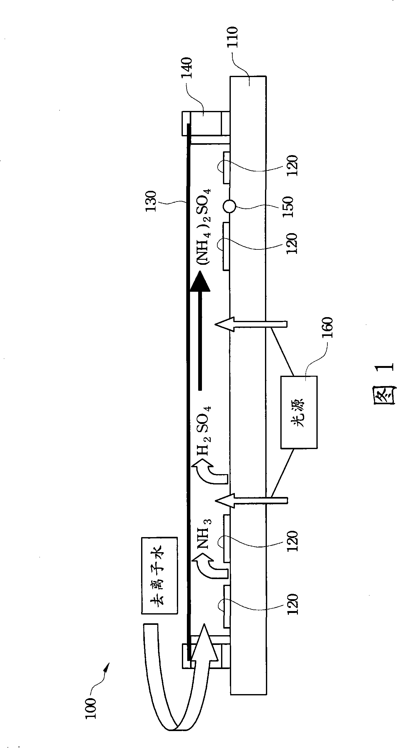
[0063] Please refer to FIG. 1 , which shows a photomask 100 with deposits such as haze contamination. In semiconductor manufacturing, the photomask 100 is used in a lithography process to transfer an image of a circuit pattern onto a semiconductor wafer. The photomask 100 can include a transparent substrate 110, and the transparent substrate 110 has fused quartz (Fused Quartz), calcium fluoride (CaF 2 ), or other suitable materials. The photomask 100 may further include an absorbing layer 120 formed on the transparent substr...


PUM


Abstract

The invention relates to a method and a system for inspecting wafers, wherein the method for inspecting semiconductor wafers which are patterned by a photomask comprises loading a first wafer and scanning a first image of the first wafer, loading a second wafer and scanning a second image of the second wafer, comparing the first and the second image, and classifying a difference detected between the first and second images as a potential defect on the photomask. The potential defect includes a haze defect on the photomask. The invention improves the defaults of the prior art, such as costliness and time-consumption, by tightly monitoring the defaults on the semiconductor wafers.

Description

technical field [0001] The present invention relates to a method and system for inspecting semiconductor wafers for defects, and more particularly, for inspecting semiconductor wafers for defects associated with reticle deposits. Background technique [0002] Photomasks (sometimes referred to as reticles) are commonly used in the lithography process of semiconductor manufacturing. Typically, a photomask is fabricated by depositing a patterned material (eg, Chromium) on one side of very flat quartz or glass. Patterned materials are used to transfer images to substrates such as semiconductor wafers. The patterned material can be selected or arranged to form a binary mask BIM (Binary Mask), a phase shift mask PSM (Phase Shift Mask), or a combination of the two to effectively pattern in the lithography process The amount of radiation projection being exposed. Since mask contamination has been a problem, high precision masks, such as those used in lithography processes with wa...

Claims


Application Information

Patent Timeline
Patent Type & Authority Applications(China)
IPC IPC(8): G01N21/956G01R31/308
CPCG03F1/84G06T7/001G06T2207/10056G06T2207/30148
Inventor 洪彰成高蔡胜
Owner TAIWAN SEMICON MFG CO LTD
Why Eureka
Try Eureka