Multi-chips package with reduced structure and method for forming the same

A technology of encapsulation structure and grain, applied in the direction of electrical components, electrical solid devices, circuits, etc., can solve problems such as complex cutting procedures, reliability problems, and sticky sand cores, and achieve low manufacturing costs, increased yields, and high reliability. sexual effect

Inactive Publication Date: 2008-08-27
ADVANCED CHIP ENG TECH INC
View PDF0 Cites 19 Cited by
  • Summary
  • Abstract
  • Description
  • Claims
  • Application Information

AI Technical Summary

Problems solved by technology

[0004] Although the use of wafer-level packaging can reduce the thermal expansion coefficient mismatch between the die and the interconnect substrate (such as the thermal expansion coefficient mismatch between the build-up layer and the redistribution layer), the silicon die (2.3) and the core paste (core paste) ( 20-180) The difference in thermal expansion coefficient is still large enough to cause the resulting mechanical stress to cause reliability problems during temperature cycle tests
In addition, the different composition and material of the cutting line, such as sand core sticky, glass and epoxy resin, will also make the cutting process more complicated
[0005] Another traditional WLP manufacturing process problem is that the stacked redistribution layers formed on the build-up layer on the die must be optimized (refined); therefore, the package thickness must be reduced to meet the shrinking package structure requirements

Method used


Image

  • Multi-chips package with reduced structure and method for forming the same
  • Multi-chips package with reduced structure and method for forming the same
  • Multi-chips package with reduced structure and method for forming the same

Examples


Embodiment Construction

[0049] The present invention will be described in detail below in conjunction with its preferred embodiments and accompanying drawings. It should be understood that all preferred embodiments in the present invention are for illustrative purposes only. Therefore, except for the preferred embodiments in the text, the present invention It can also be widely applied in other embodiments. And the present invention is not limited to any embodiment, but should be determined by the scope of the appended claims and their equivalent fields.

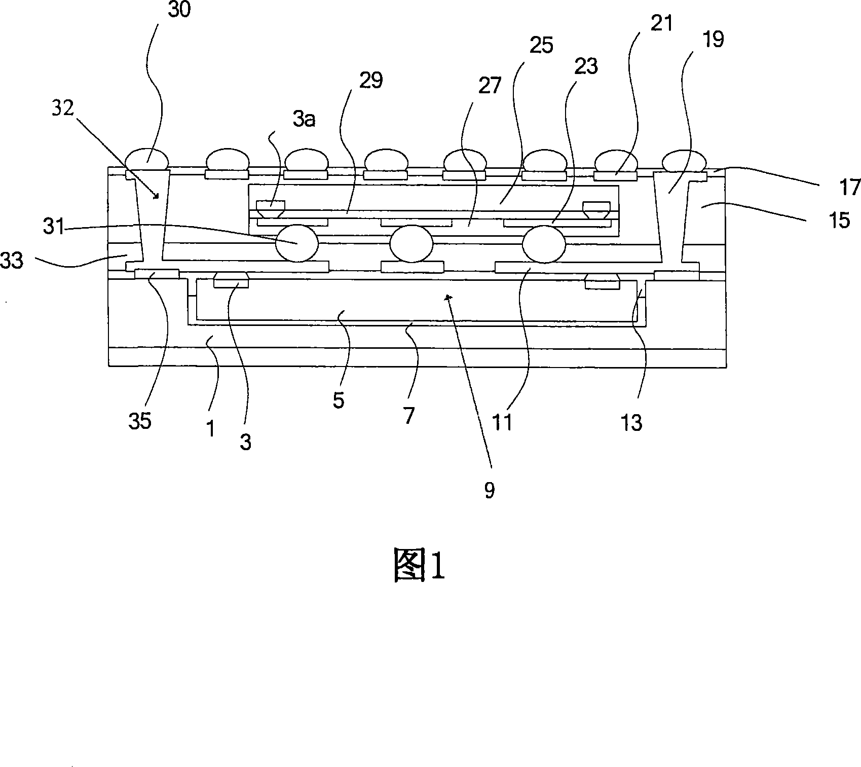
[0050] The invention discloses a fan-out wafer level packaging structure, which includes a substrate, wherein the substrate includes a pre-formed hole substrate and metal pads formed thereon. FIG. 1 shows a cross-sectional view of a board-level package (PSP) structure for a system-in-package (SIP) in an embodiment of the present invention. As shown in Figure 1, the system-in-package structure includes a substrate 1, and the substrate 1 includes a ...


PUM


Abstract

The present invention provides a structure of multi-chips package and method of the same comprising a substrate with a pre-formed die receiving cavity formed within an upper surface of the substrate. A die is disposed within the die receiving cavity by adhesion and an elastic dielectric layer filled into a gap between the die and the substrate to absorb thermal mechanical stress; therefore the thickness of the package is reduced and the CTE mismatch of the structure is reduced. The present invention also provides a structure for SIP with higher reliability and lower manufacturing cost. the process is simpler and it is easy to form the multi-chips package than the traditional one. Therefore, the present invention discloses a fan-out WLP with reduced thickness and good CTE matching performance.

Description

technical field [0001] The present invention relates to system-in-package (SIP), more specifically to board-level package (PSP) of system-in-package, and in particular to a multi-die package structure with reduced structure and its forming method. Background technique [0002] In the field of semiconductor devices, the device size is reduced but the device density is increased. Traditional packaging technologies, such as lead frame packaging, flexible packaging, and rigid packaging technology cannot meet the needs of manufacturing small-sized dies with high cell density; therefore, there is a demand for new packaging and in-line technologies suitable for high-density cells. [0003] For the above reasons, packaging technology is developing towards ball grid array packaging (BGA), flip chip (FC-BGA), grain level packaging (CSP), and wafer level packaging (WLP); among them, wafer level packaging is an advanced packaging technology , The packaging and testing of the die is per...

Claims


Application Information

Patent Timeline
Patent Type & Authority Applications(China)
IPC IPC(8): H01L25/00H01L25/065H01L23/48H01L21/50H01L21/60
CPCH01L2924/09701H01L2224/24227H01L2924/15153H01L2224/16145H01L2224/73267H01L25/0657H01L2224/92244H01L2225/06524H01L2924/0002H01L2224/12105H01L2225/06527H01L2225/06541H01L24/19H01L25/50H01L2924/10253H01L23/13H01L2225/06513H01L25/0652H01L2224/32225H01L2924/351H01L2224/05026H01L2224/05548H01L2224/05001H01L2224/05124H01L2224/05147H01L2224/05155H01L2224/05166H01L2224/05644H01L2224/05666H01L2924/00H01L2924/00014H01L2924/01029H01L2924/01079H01L2924/01055H01L23/12
Inventor 杨文焜许献文吴雅慈黄清舜
Owner ADVANCED CHIP ENG TECH INC
Why Eureka
Try Eureka