Method for the production of a semiconductor component comprising a planar contact, and semiconductor component

A semiconductor and device technology, applied in the field of semiconductor devices, can solve problems such as thermal resistance limitations

Inactive Publication Date: 2008-08-27
OSRAM OPTO SEMICON GMBH & CO OHG
View PDF2 Cites 5 Cited by
  • Summary
  • Abstract
  • Description
  • Claims
  • Application Information

AI Technical Summary

Problems solved by technology

However, with conventional barrier films, thermal, aging or UV resistance is partially limited

Method used


Image

  • Method for the production of a semiconductor component comprising a planar contact, and semiconductor component

Examples


Embodiment Construction

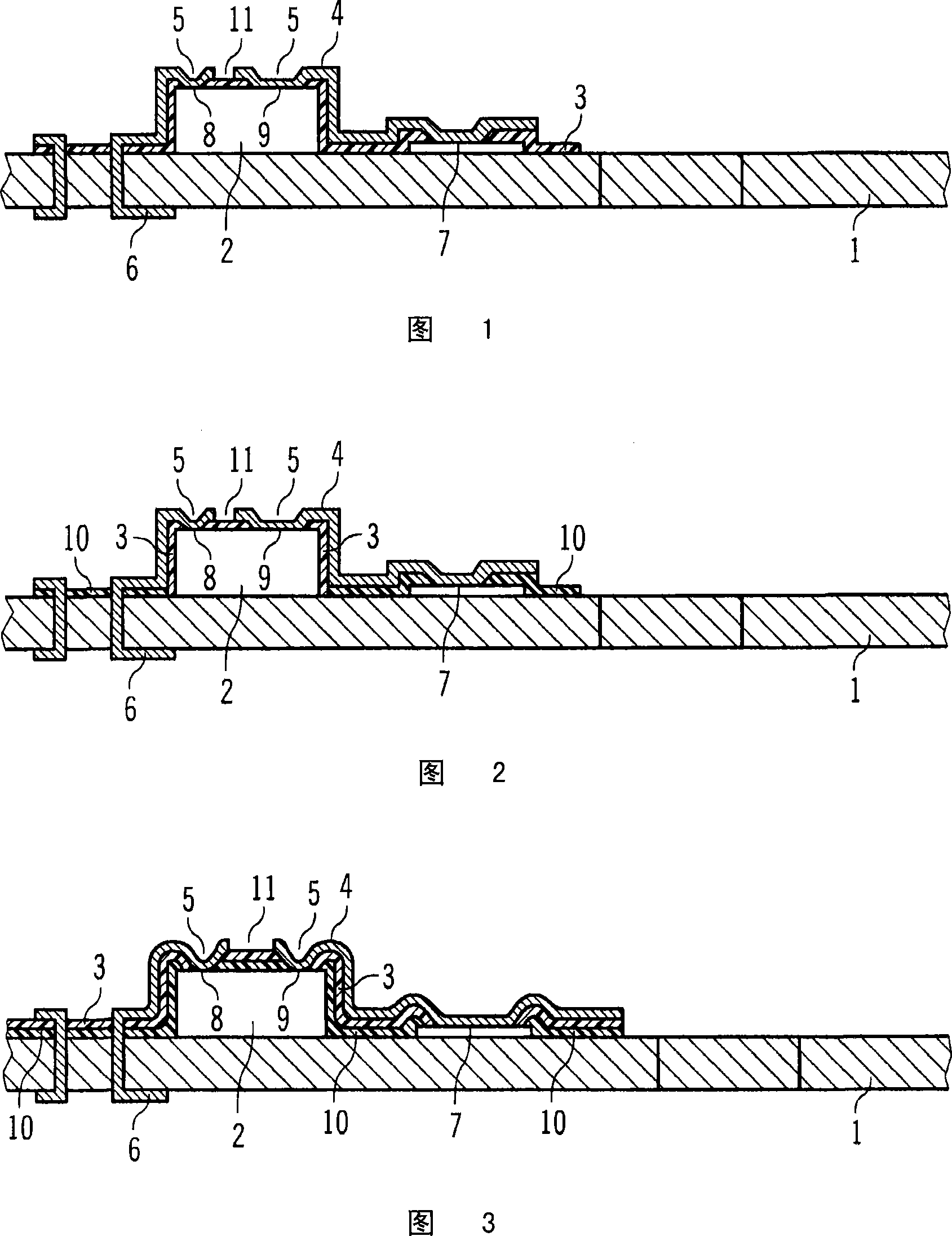
[0028] FIG. 1 shows a semiconductor device in which an LED chip 2 is arranged on a substrate 1 . The substrate 1 can be, for example, a wafer, a printed circuit board (PCB) and / or a flexible material (flex material).

[0029] An insulating layer 3 of glass, for example a thin layer of borosilicate glass, is applied on the substrate 1 and on the LED chip 2 . This borosilicate glass layer serves both as a thermal protection layer for the LED chip 2 and as a thermal protection layer for the substrate 1 . The glass coating 3 thus protects the LED chip 2 and the substrate 1 from environmental influences such as moisture, dust or radiation.

[0030] The insulating layer 3 also serves for the electrical insulation between subregions of the LED 2 , in particular the sides of the LED chip 2 , and the electrical connection 4 for the areal electrical contacting of the LED chip. A planar contact is to be understood here as a wireless contact formed by means of a structured metal layer w...


PUM


Abstract

The invention relates to a method for producing a semiconductor component, especially a semiconductor structure having a surface structure or topography created on a substrate (1) by means of electronic components (2). According to said method, one or several electronic components (2) are applied to a substrate (1), and an insulation layer (3) is applied to the topography created on the substrate (1) by means of the at least one component (2). Contacting holes (5) are then created at contact points (8, 9) of the at least one electronic component in the insulation layer (3), the insulation layer (3) and the contact points (8, 9) are plated in the contacting holes (5), and the plating is structured to create electrical connections (4). The insulation layer (3) is provided with a glass coating.

Description

technical field [0001] The invention relates to a method according to the preamble of claim 1 and to a semiconductor device produced by means of this method. [0002] This patent application claims priority from German patent application 102005041099.5, the disclosure of which is hereby incorporated by reference. Background technique [0003] In the planar bonding process known from WO 03 / 030247 A2, which is also referred to as the SiPLIT process, the component is surrounded by a thin film with a predetermined layer thickness that is uniformly superimposed on the topography and forms an insulating layer. The basic principle of the planar construction with planar connection technology enables a wide variety of application-specific construction possibilities through the use of insulating films. [0004] Traditionally, transparent potting materials or barrier films are currently used to cover components. However, when conventional barrier films are used, the thermal, aging or...

Claims


Application Information

Patent Timeline
Patent Type & Authority Applications(China)
IPC IPC(8): H01L23/051H01L23/482H01L33/00H01L33/44H01L33/62
CPCH01L23/482H01L23/5389H01L24/24H01L24/82H01L25/0655H01L33/44H01L33/62H01L2224/24011H01L2224/24051H01L2224/24226H01L2224/24998H01L2224/82039H01L2224/82047H01L2924/01015H01L2924/01033H01L2924/01078H01L2924/12044H01L2924/01005H01L2924/01006H01L2924/01019H01L2224/82007H01L2924/351H01L2924/00H01L23/051
Inventor K·韦德纳
Owner OSRAM OPTO SEMICON GMBH & CO OHG
Why Eureka
Try Eureka