Making method for circuit board

A manufacturing method and circuit board technology, which can be used in multilayer circuit manufacturing, circuits, semiconductor/solid-state device manufacturing, etc., can solve problems such as undisclosed circuit layers, and achieve the effect of increasing wiring density

Active Publication Date: 2008-09-10
ADVANCED SEMICON ENG INC
View PDF2 Cites 2 Cited by
  • Summary
  • Abstract
  • Description
  • Claims
  • Application Information

AI Technical Summary

Problems solved by technology

However, the above-mentioned US patent does not disclose that the contact 315 of the semiconductor element 312 (ie, the embedded element) is electrically connected to the circuit layer of the circuit board.

Method used


Image

  • Making method for circuit board
  • Making method for circuit board
  • Making method for circuit board

Examples


Embodiment Construction

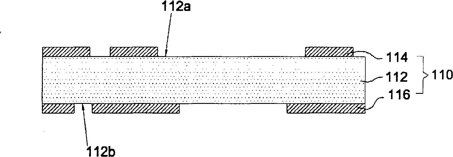
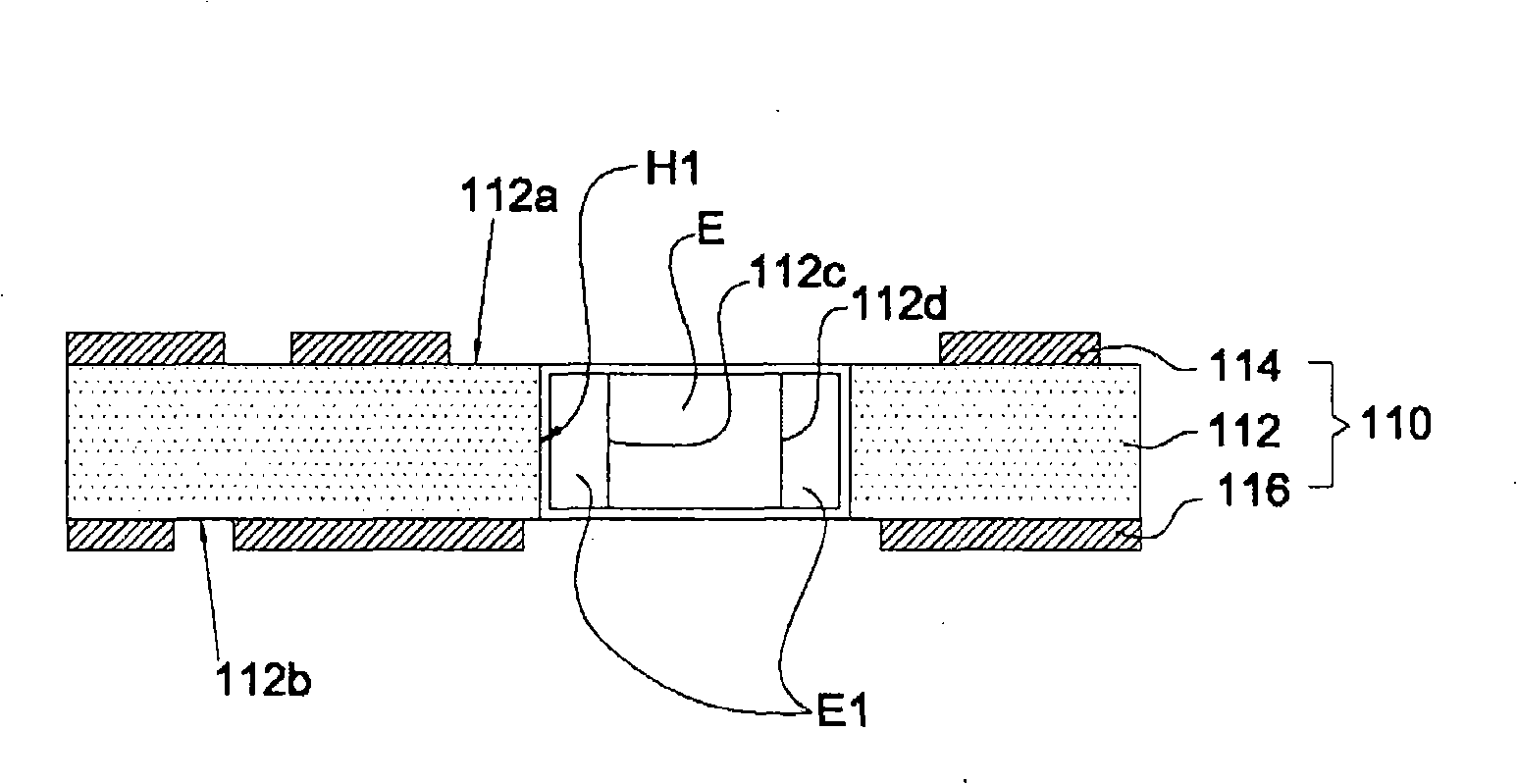
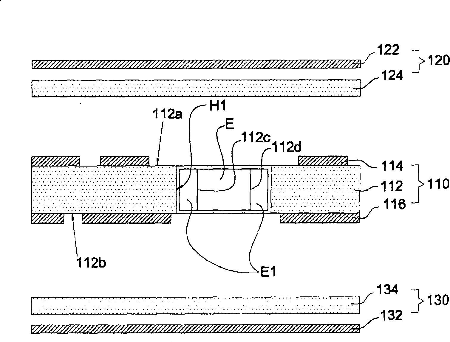
[0098] refer to Figure 8 , which shows the manufacturing method of the circuit board with embedded components according to the first embodiment of the present invention. refer to Figure 9 , in step 402, a core layer 510 is provided, which includes a first dielectric layer 512 and first and second metal layers 514, 516, wherein the first dielectric layer 512 has an upper surface 512a and a lower surface 512b , the first and second metal layers 514 , 516 are respectively located on the upper surface 512 a and the lower surface 512 b of the first dielectric layer 512 . In this embodiment, the material of the first and second metal layers 514 and 516 may be copper, and the thickness thereof may be equal to or less than 3 micrometers (μm).

[0099] refer to Figure 10 , in step 404 , a first through hole 511 is formed in the core layer 510 . For example, a first through hole 511 can be formed in the core layer 510 by mechanical drilling or laser hole forming process. In this...


PUM


Abstract

The embodiment of the invention provides a manufacturing method of a circuit board, which comprises the steps as follows: a core layer is provided, which comprises a first dielectric layer, a first metal layer and a second metal layer; a through hole is formed on the core layer; the core layer is arranged on a support board, an in-built element is arranged in the through hole, the second metal layer contacts with the support board, the in-built element is provided with at least one electrode contact, which contacts with the support board; the in-built element is fixed in the through hole; the support board is removed; the first metal layer and the second metal layer are removed, the thickness of the electrode contact of the in-built element is lessened; a third metal layer and a fourth metal layer are formed respectively, wherein, the fourth metal layer is electrically connected with the electrode contact of the in-built element; the third metal layer and the fourth metal layer are patterned, thereby forming a first patterned wiring layer and a second patterned wiring layer. The embodiment of the invention can lessen the thickness of an electrode contact of an in-built element through a reduction technique.

Description

technical field [0001] The invention relates to a method for manufacturing a circuit board, more particularly to a method for manufacturing a circuit board with embedded components, which can reduce the thickness of the electrode contacts of the embedded components through a thickness reduction process. Background technique [0002] The known circuit board is mainly composed of multiple layers of patterned circuit layers and dielectric layers laminated alternately. Wherein, the patterned circuit layer is defined and formed by a copper foil layer (copperfoil) through photolithography and etching process, and the dielectric layer is arranged between the patterned circuit layers to isolate two adjacent patterned circuit layers. In addition, adjacent patterned circuit layers are electrically connected to each other through plating through holes (PTH) or conductive vias penetrating the dielectric layer. Finally, arrange various electronic components (such as active components or...

Claims


Application Information

Patent Timeline
IPC IPC(8): H05K3/46H05K3/30H05K3/40H01L21/50H01L21/56H01L21/60H01L21/48
CPCH01L2224/04105H01L2224/19H01L2224/2518H01L2924/3512
Inventor 王永辉欧英德
Owner ADVANCED SEMICON ENG INC
Why Eureka
Try Eureka