Display apparatus, display apparatus driving method and electronic equipment

A technology for display devices and scanning devices, which is applied in lighting devices, logic circuit coupling/interfaces, and circuits using field effect transistors, and can solve problems such as loss of uniformity of the screen and achieve high-quality display images

Inactive Publication Date: 2008-09-17
JOLED INC
View PDF1 Cites 30 Cited by
  • Summary
  • Abstract
  • Description
  • Claims
  • Application Information

AI Technical Summary

Problems solved by technology

Therefore, the screen loses uniformity

Method used


Image

  • Display apparatus, display apparatus driving method and electronic equipment
  • Display apparatus, display apparatus driving method and electronic equipment
  • Display apparatus, display apparatus driving method and electronic equipment

Examples


no. 1 example

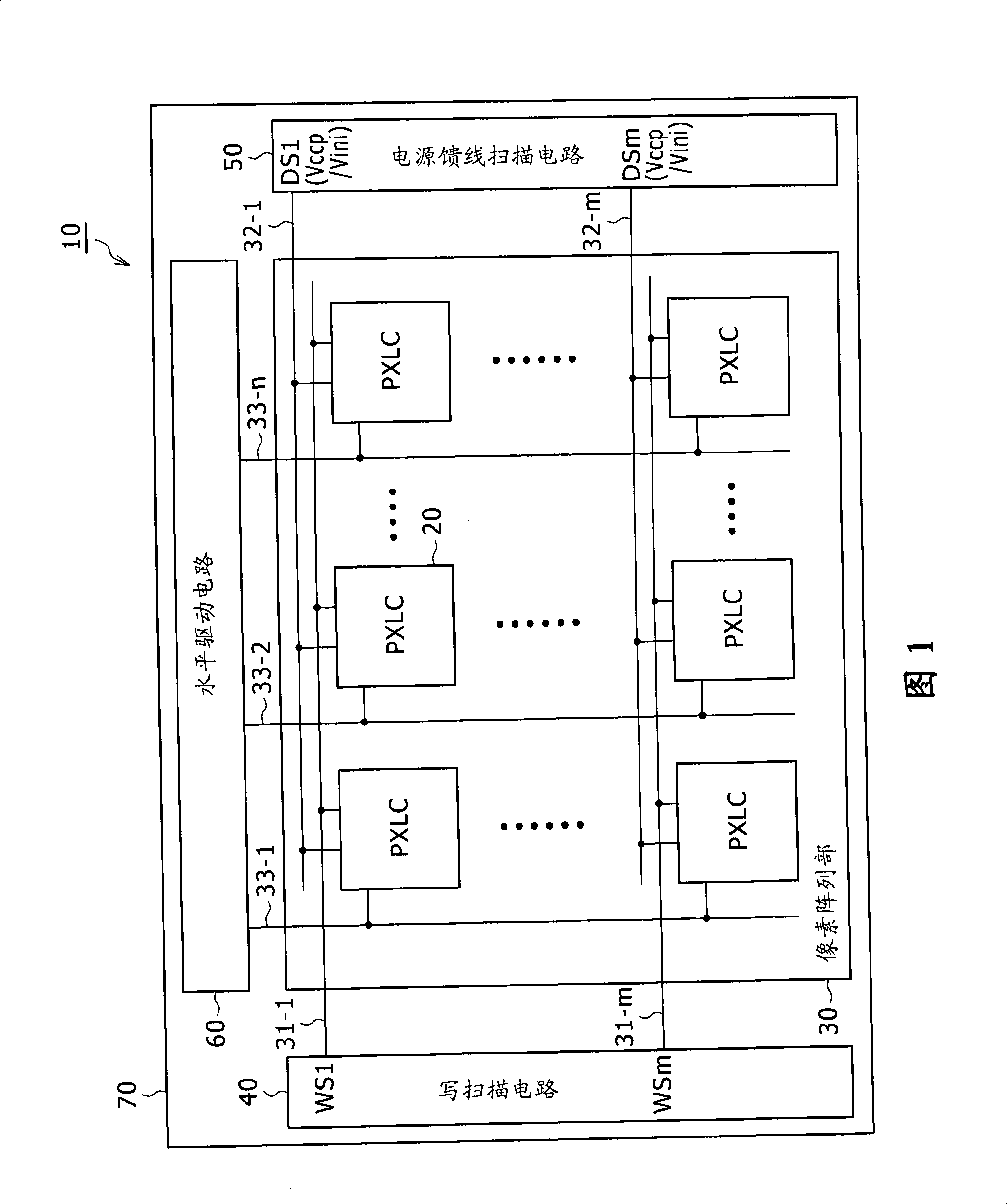
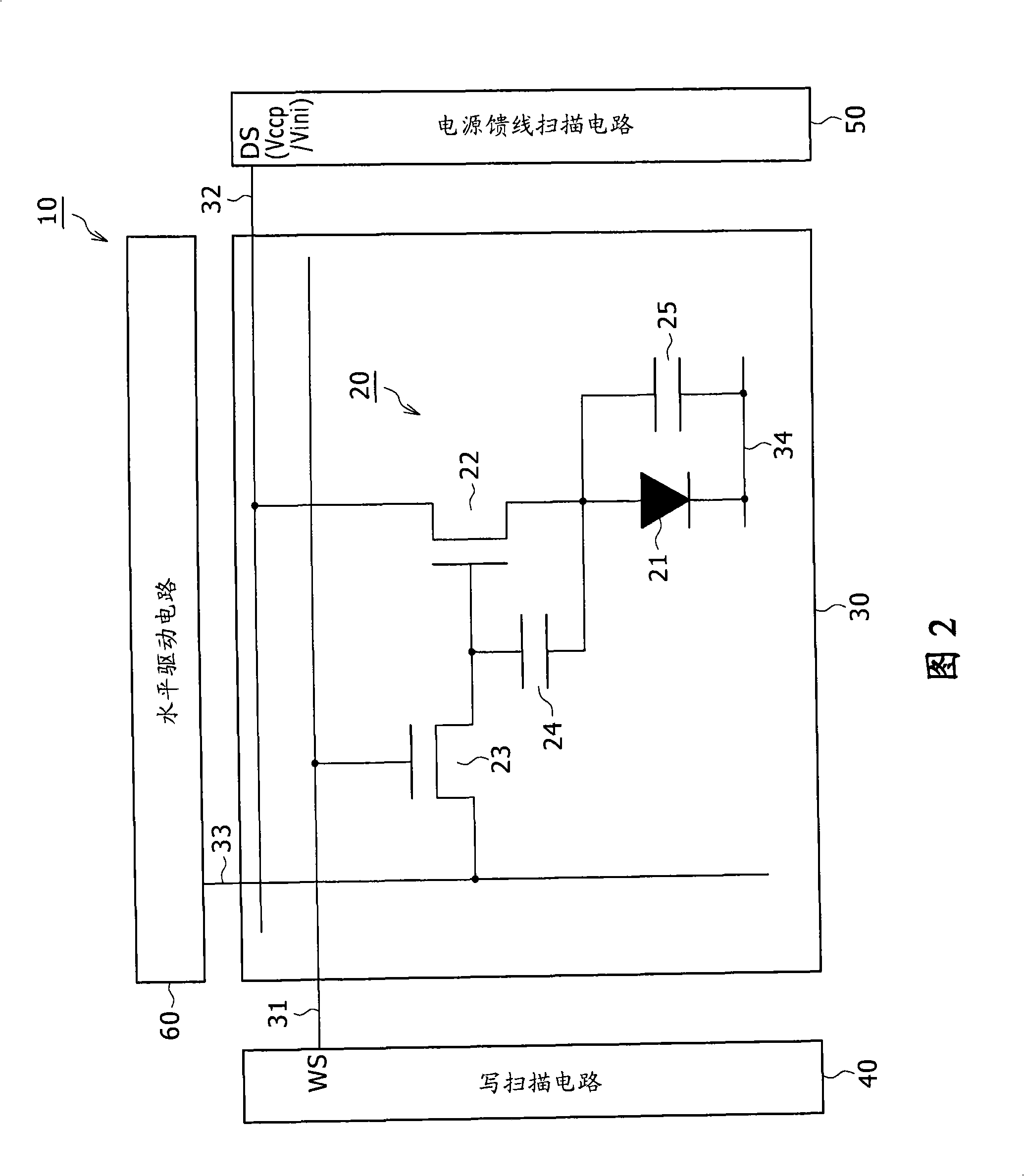
[0149] Figure 10 is a circuit diagram showing a typical configuration of the control device according to the first embodiment. As shown, the control device employs a last-stage buffer 50A connected to the power feeder 32 (ie, any one of the power feeders 32-1 to 32-m). The final-stage buffer 50A is a portion included in the power feeder scanning circuit 50 as a portion connected to the power feeder 32 connected to the pixel row of the pixel array section 30 .

[0150] The final-stage buffer 50A has a CMOS inverter configuration including a P-channel MOS transistor P11 and an N-channel MOS transistor N11. The source of the P-channel MOS transistor P11 is connected to a power supply line of a high first potential Vccp. The source of the N-channel MOS transistor N11 is connected to the power supply line of the low second potential Vini. The drain of the P-channel MOS transistor P11 is connected to the drain of the N-channel MOS transistor N11 through the drain common connecti...

no. 2 example

[0161] Figure 12 is a circuit diagram showing a typical configuration of the control device according to the second embodiment. Figure 12 shown with Figure 10 Elements that are the same as each corresponding element shown are denoted by the same symbols as the corresponding elements. Such as Figure 12 As shown, the control device employs a final stage buffer 50B connected to the power feeder 32 (ie, any one of the power feeders 32-1 to 32-m). The final-stage buffer 50B is a portion included in the power feeder scanning circuit 50 as a portion connected to the power feeder 32 connected to the pixel row of the pixel array section 30 .

[0162] The final-stage buffer 50B has a clocked inverter configuration including a P-channel MOS transistor P11, a P-channel MOS transistor P12, an N-channel MOS transistor N11, and an N-channel MOS transistor N12. The source of the P-channel MOS transistor P11 is connected to a power supply line of a high first potential Vccp. The sourc...

no. 3 example

[0175] Figure 14 is a circuit diagram showing a typical configuration of the control device according to the third embodiment. As shown in the drawing, the control device employs a final-stage buffer 50C connected to the power feeder 32 (ie, any one of the power feeders 32-1 to 32-m). The final-stage buffer 50C is a portion included in the power supply line scanning circuit 50 as a portion connected to the power supply line 32 connected to the pixel row of the pixel array section 30 .

[0176] The final-stage buffer 50C has a two-phase input inverter configuration including a P-channel MOS transistor P13 and an N-channel MOS transistor N13. The source of the P-channel MOS transistor P13 is connected to the power supply line of the high first potential Vccp. The source of the N-channel MOS transistor N13 is connected to the power supply line of the low second potential Vini. The drain of the P-channel MOS transistor P13 is connected to the drain of the N-channel MOS transis...


PUM


Abstract

In the present invention, there is provided a display apparatus including: a pixel array section including pixel circuits each having an electro-optical device, a write transistor configured to carry out a voltage storing process, a holding capacitor configured to hold the sampled video signal, and a driving transistor configured to drive the electro-optical device; first scan means for carrying out a selective scan operation in row units and driving each of the write transistors; second scan means for selectively supplying either a first or second electric potential synchronously with the selective scan operation for feeding a current to each of the driving transistors; and control means for sustaining a power-supply feed line in a floating state during a period ending at a time not earlier than the start of the voltage storing process after a voltage corresponding to the threshold voltage of the driving transistor has been held in the holding capacitor.

Description

[0001] Cross References to Related Applications [0002] This application contains subject-matter of Japanese Patent Application JP 2007-068003 filed in the Japan Patent Office on Mar. 16, 2007, the entire content of which is hereby incorporated by reference. technical field [0003] The present invention relates to a display device, a method for driving the display device, and electronic equipment. More specifically, the present invention relates to a flat-panel type display device in which pixel circuits each including a photoelectric element undergo The arrangement forms a matrix. Background technique [0004] In recent years, in the field of display devices for displaying images, flat panel type display devices in which pixels (pixel circuits) each including a light emitting element are arranged to form a matrix have rapidly spread. A light-emitting element included in each pixel circuit in a flat-panel display device is a so-called current-driven type photoelectric el...

Claims


Application Information

Patent Timeline
Patent Type & Authority Applications(China)
IPC IPC(8): G09G3/30G09G3/20H01L51/50H03K19/0185
CPCG09G3/3233G09G3/3291G09G2300/0819G09G2300/0842G09G2300/0866G09G3/30G09G3/32G09G3/20H05B33/12
Inventor 谷龟贵央饭田幸人三并徹雄内野胜秀
Owner JOLED INC
Why Eureka
Try Eureka