A method for selectively etching silicon nano line

A silicon nanowire, selective technology, applied in nanotechnology, nanotechnology, nanostructure manufacturing and other directions, can solve the problems of high cost, complex process, incapable of mass production, etc., and achieve the effect of low cost, simple and reliable process

Inactive Publication Date: 2008-09-17
EAST CHINA NORMAL UNIV
View PDF0 Cites 32 Cited by
  • Summary
  • Abstract
  • Description
  • Claims
  • Application Information

AI Technical Summary

Problems solved by technology

[0004] The purpose of the present invention is to provide a method for selectively etching silicon nanowires in view of the defects in the prior art and market demand, so as to solve the complex process, high cost and inability to batch the existing silicon nanowire electrodes. production problem

Method used


Image

  • A method for selectively etching silicon nano line
  • A method for selectively etching silicon nano line
  • A method for selectively etching silicon nano line

Examples


Embodiment

[0015] The method for selectively etching silicon nanowires of the present invention comprises the following sequential steps:

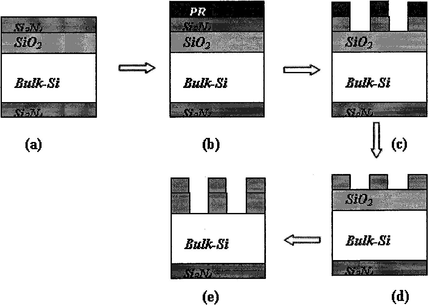
[0016] a) Using "top-down" standard microelectronics processing technology to open windows on the surface of silicon wafers

[0017] Use P(100) double-sided polished silicon wafers, according to figure 1 The process flow shown opens a window on the surface of the silicon wafer, that is, patterning:

[0018] ①Mask-First, use the method of oxidation to thermally oxidize a layer of silicon dioxide on the front and back sides of the silicon wafer, with a thickness of Secondly, use atmospheric pressure chemical vapor deposition to vapor-deposit silicon nitride on both sides of the silicon wafer, with a thickness of

[0019] ②Use photolithography to transfer the pattern on the mask to the surface of the silicon wafer;

[0020] ③Use plasma to remove silicon nitride on one side of the silicon wafer;

[0021] ④Remove silicon dioxide with silicon dioxid...


PUM


Abstract

The invention discloses a method for selectively etching silicon nano-wire according to defects in existing technology and market requirement, comprising: a) using ''up to down'' standard microelectronic manufacturing process to open a window on a silicon sheet; b) using ''up to down'' non-electroplating chemical deposition method to etch silicon nano-wires on surface of the silicon sheet with opened window. Compared to the existing technology, the method for selectively etching silicon nano-wire according to the invention can not only make any expected image, but also obtain uniformly arranged silicon nano-wire array with regular size; also it has the advantages of simple manufacturing process, low costs, suitable for batch production, to realize industrial manufacture of silicon nano-wire electrode, and provide a scheme manufacturing nano-electric element based on a plurality of nano-wires.

Description

technical field [0001] The invention relates to a method for selectively etching silicon nanowires, which belongs to the technical field of nanomaterial preparation. Background technique [0002] Silicon nanowires have attracted widespread attention due to their unique optical and electrical properties such as quantum confinement effects, quantum tunneling effects, and Coulomb blockade effects, as well as high surface activity. Silicon nanowires are widely used in nanoelectronic devices such as nanosensors, single-electron transistors, and single-electron storage, as well as in the synthesis of other nanomaterials. It can become a new material with great application potential in the field of nanoelectronics. If practical nanoelectronic devices can be prepared with silicon nanowires, the application of silicon technology will be extended from the field of microelectronics to the field of nanoelectronics, which will have an immeasurable impact on the development of future elec...

Claims


Application Information

Patent Timeline
Patent Type & Authority Applications(China)
IPC IPC(8): H01L21/00H01L21/02H01L21/20H01L21/28B82B3/00
Inventor 万丽娟龚文莉陶伯睿蒋珂玮李辉麟张健
Owner EAST CHINA NORMAL UNIV
Why Eureka
Try Eureka