System for processing thin-film material surface using bi-medium to block electric discharge

A thin-film material, barrier discharge technology, applied in electrical components, plasma, etc., can solve the problems of affecting the surface properties of materials, ablation, and large local micro-arc current, and achieve the effect of avoiding uneven heating

Inactive Publication Date: 2008-10-01
ACAD OF OPTO ELECTRONICS CHINESE ACAD OF SCI +1
View PDF0 Cites 12 Cited by
  • Summary
  • Abstract
  • Description
  • Claims
  • Application Information

AI Technical Summary

Problems solved by technology

[0003] The dielectric barrier discharge in the air generally places an insulating medium between the two electrodes. The discharge is directly punctured air, and the local micro-arc current generated by the discharge is relatively large. When it is used to pr

Method used


Image

  • System for processing thin-film material surface using bi-medium to block electric discharge
  • System for processing thin-film material surface using bi-medium to block electric discharge
  • System for processing thin-film material surface using bi-medium to block electric discharge

Examples


Embodiment Construction

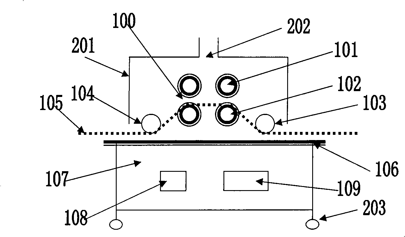
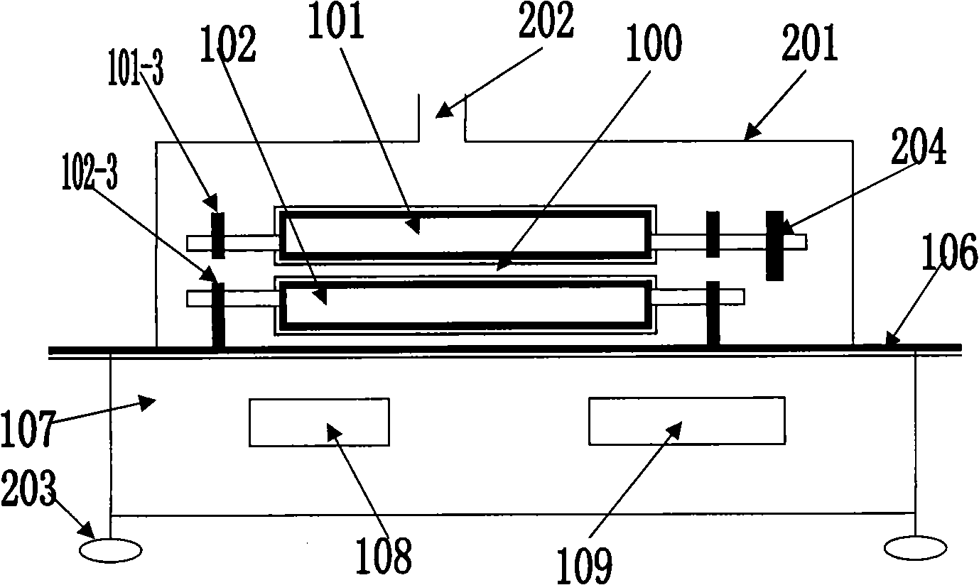
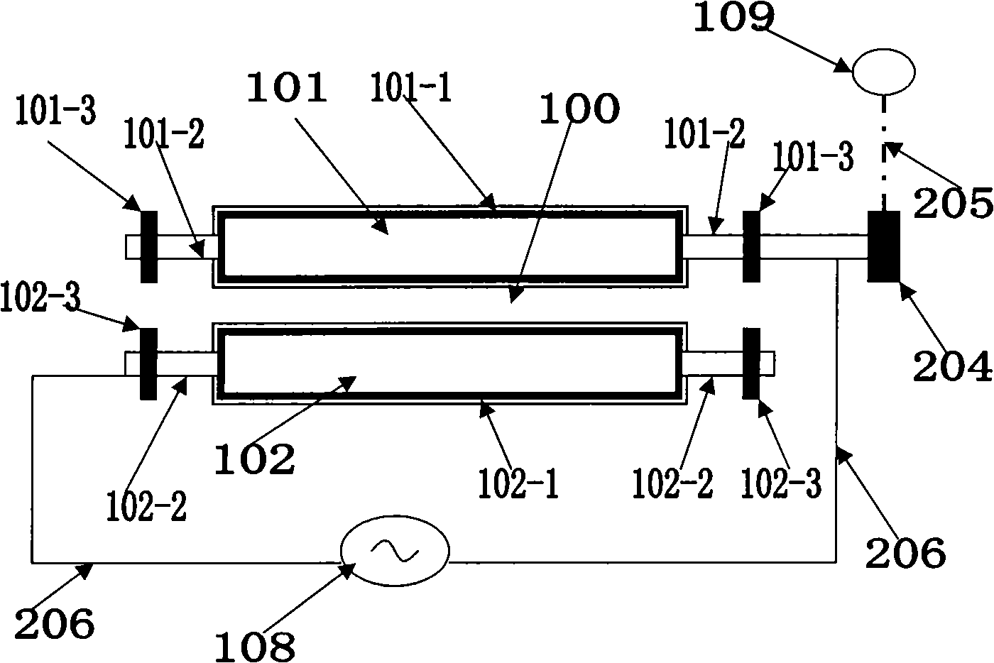
[0017] The present invention will be described in detail below in conjunction with specific embodiments with reference to the accompanying drawings. refer to figure 1 and figure 2 , are respectively the front structure schematic diagram and the side structure schematic diagram of the embodiment of the present invention; as figure 1 and figure 2 As shown, the double-dielectric barrier discharge treatment device for the surface of thin film materials includes a housing 107 for installing a high-frequency and high-voltage power supply 108. On the upper panel 106 of the housing, there are multiple groups of parallel glass tubes or ceramic tubes. The upper metal tube electrode 101 and the lower metal tube electrode 102 with the same gap between them, wherein the upper metal tube electrode 101 is driven by a motor 109 to rotate, and the lower metal tube electrode 102 is driven by the film material 105 to form a rotation. When the film material 105 passes through the upper and lo...


PUM


Abstract

The present invention provides a system of processing film material surface by a dual dielectric barrier discharge, including a high frequency power supply, a motor, discharge electrodes and an electrode casing, the discharge electrodes are composed by upper and lower metal tube electrodes which are multi-group parallel, covered by glass tubes or ceramic tubes and has same gap between electrodes, the two insulation material tubes covering the upper and lower metal tube electrodes form a dual dielectric between electrodes, the two ends of the upper and the lower electrode tubes are connected with a bearing respectively, the upper electrode tube is rotary driven by the motor, the lower electrode tube is rotary driven by the film penetrating through two electrodes, the upper and the lower metal tubes are connected with the high frequency power supply respectively, the upper and lower electrode tubes are placed in one casing, when the film material penetrates through the upper and lower metal tube electrodes, the surface is processed with modification treatment by plasma.

Description

technical field [0001] The invention relates to a system for treating the surface of thin film materials by double-dielectric barrier discharge, especially refers to a system in which multiple groups of metal tube electrodes are respectively covered with glass tubes or ceramic tubes, and the electrodes rotate by themselves when the discharge is in progress, and can pass through between the electrodes. Discharge device for thin film materials. Background technique [0002] Plasma technology has only been developed rapidly in recent years and has been widely used. For example, it can be used for: (1) Silicon wafer cleaning in the microelectronics industry, replacing the current acid and deionized water cleaning. (2) Clean all biologically and chemically contaminated surfaces, including surfaces and spaces contaminated by biological and chemical weapons. (3) Instead of wet chemical method, it can be used for in-situ disinfection in pharmaceutical and food industries. (4) Used...

Claims


Application Information

Patent Timeline
IPC IPC(8): H05H1/24H05H1/34C23F4/00
Inventor 王守国
Owner ACAD OF OPTO ELECTRONICS CHINESE ACAD OF SCI
Why Eureka
Try Eureka