

Semiconductor memory device
一种存储器件、半导体的技术,应用在静态存储器、数字存储器信息、信息存储等方向,能够解决动作容限减少等问题
Inactive Publication Date: 2008-10-15
PANASONIC CORP
View PDF1 Cites 7 Cited by
- Summary
- Abstract
- Description
- Claims
- Application Information
AI Technical Summary
Problems solved by technology
However, when many memory blocks are activated at the same time, there is a limit to the maximum number of word lines that can be activated at the same time due to a power supply voltage drop or noise caused by an increase in the instantaneous current.
Method used
View moreImage
Smart ImageViewing Examples

Examples
Embodiment 1
Embodiment 2
Embodiment 3
Login to View More PUM
 Abstract
A semiconductor memory device includes a plurality of memory blocks, a plurality of refresh block counters, a refresh word line counter, and an arbitration circuit. The plurality of refresh block counters generate block addresses of at least two memory blocks to select at least two memory blocks to be refreshed from the plurality of memory blocks. The refresh word line counter generates a common word line address that is common to the at least two memory blocks. The arbitration circuit generates at least one first word line address based on the at least two block addresses and the common word line address and arbitrate so that each word line indicated by the at least one first word line address is refreshed during a period in which a word line indicated by an externally applied second word line address is accessed.
Description
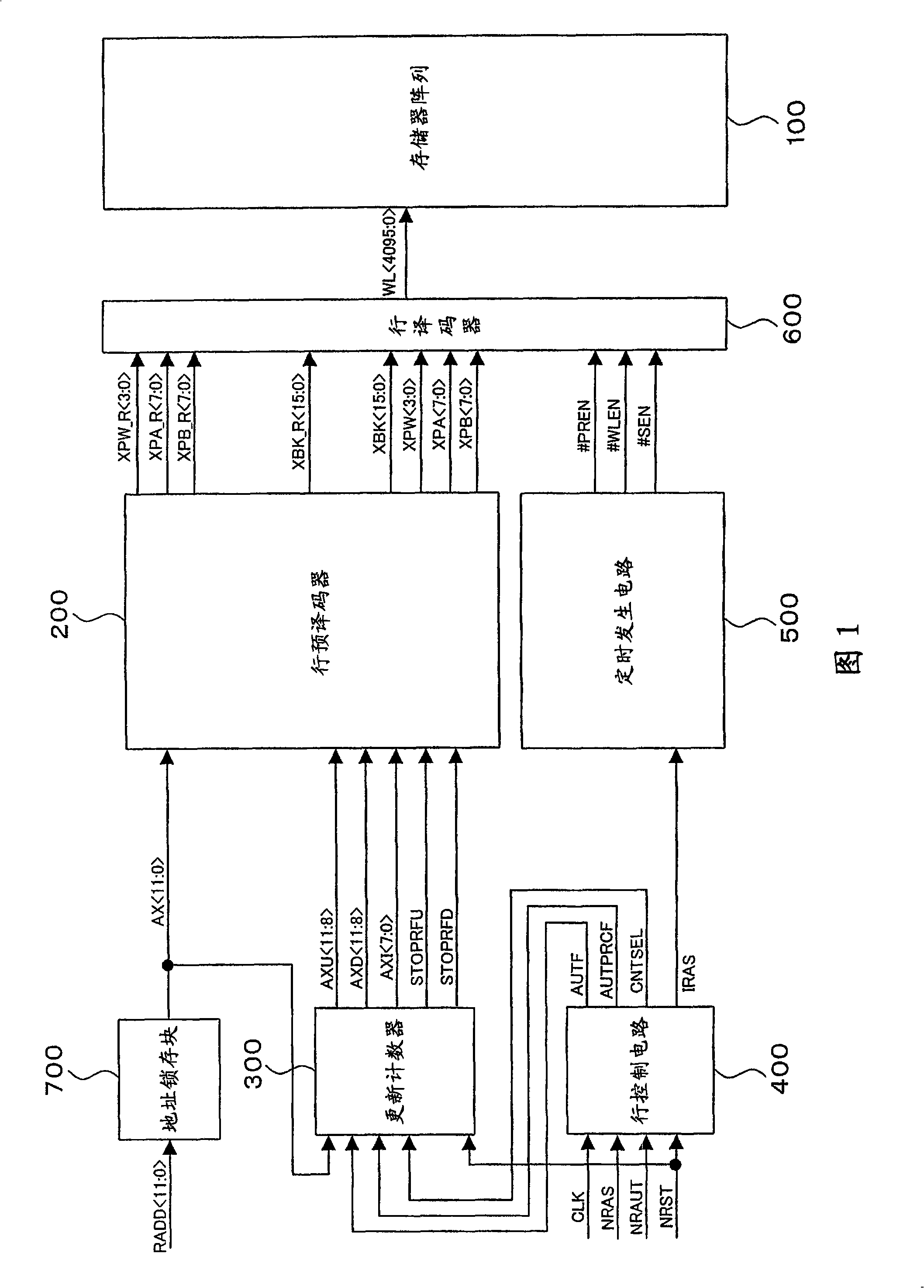
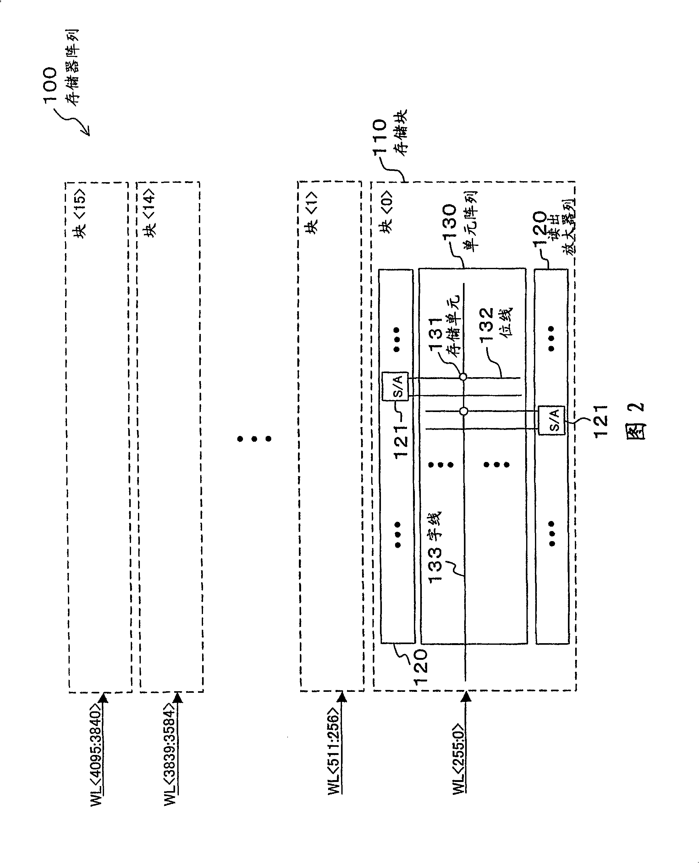
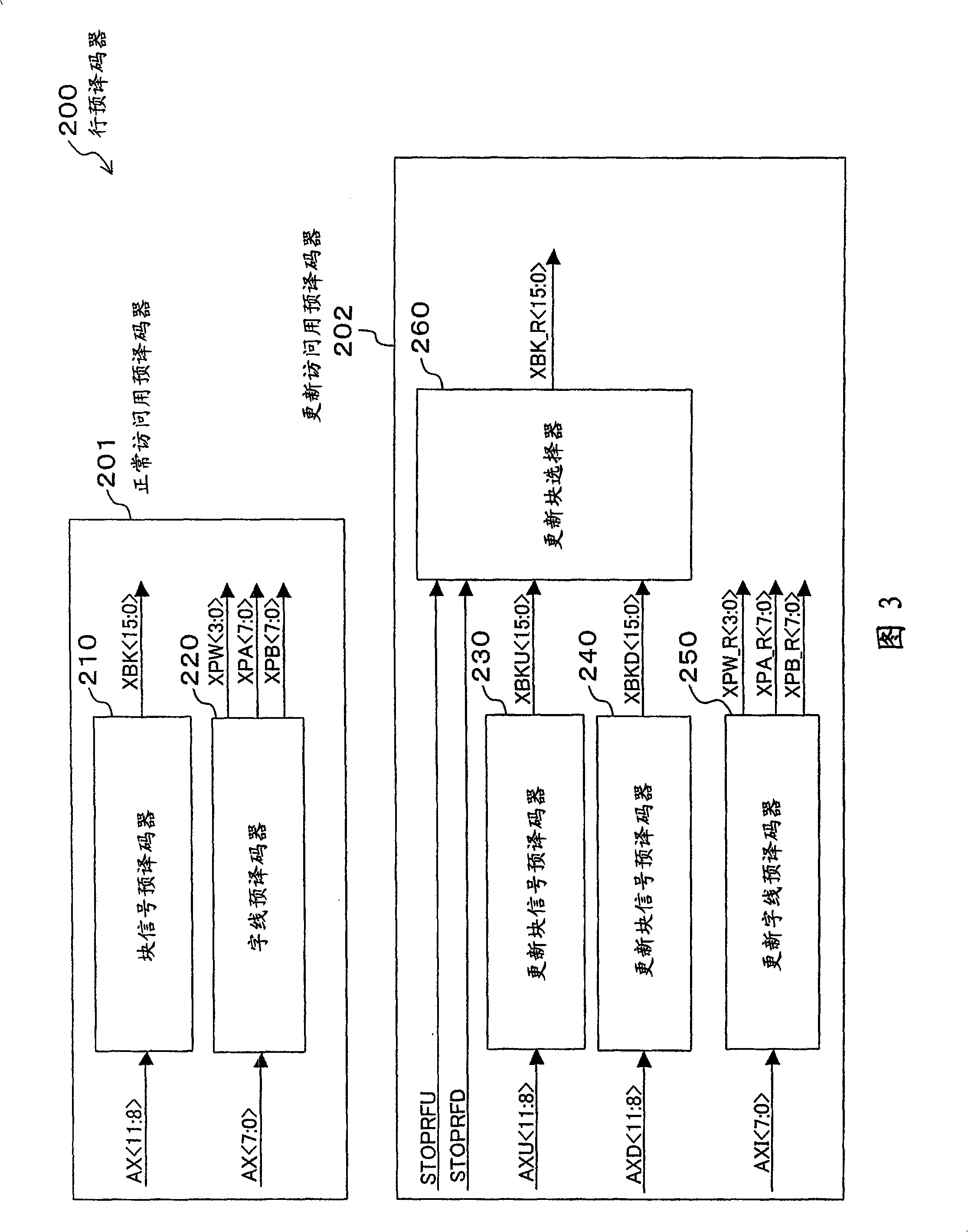
Semiconductor memory device technical field The present invention relates to a semiconductor memory device, and in particular, to an update operation of a DRAM (Dynamic Random Access Memory: Dynamic Random Access Memory). Background technique In recent years, in order to realize SOC (System On Chip) at low cost, high integration is required for DRAM for hybrid loading. Occupying most of the memory area is a memory array having a plurality of memory cells. Heretofore, in order to realize high integration, miniaturization of memory cell area has been carried out by miniaturization technology of memory cell transistors or storage capacitors using high dielectric constant insulating films. For example, in the case of a stack type memory cell, a new high-permittivity insulating film is introduced to ensure capacitor capacitance against the reduction in capacitor area due to miniaturization. However, in order to increase the capacitor capacitance of the memory cell, it is nec...
Claims
Login to View More Application Information
Patent Timeline
 Patent Type & AuthorityApplications(China)
IPC IPC(8): G11C11/406
CPCG11C11/406G11C11/40603G11C11/40618
Inventor饭田真久大田清人
OwnerPANASONIC CORP