Method for processing outer casing of bulk amorphous alloy electronic product and processing device
A technology for amorphous alloys and electronic products, which is applied in the field of processing methods and processing devices for bulk amorphous alloy electronic product shells, and can solve the problem of product performance that is difficult to meet higher load-bearing requirements, casting defects that are difficult to eliminate, and wall thickness that cannot be exceeded Thin and other problems, to achieve the effect of simple structure, uniform heating and convenient operation
- Summary
- Abstract
- Description
- Claims
- Application Information
AI Technical Summary
Problems solved by technology
Method used
Image
Examples
Embodiment 1
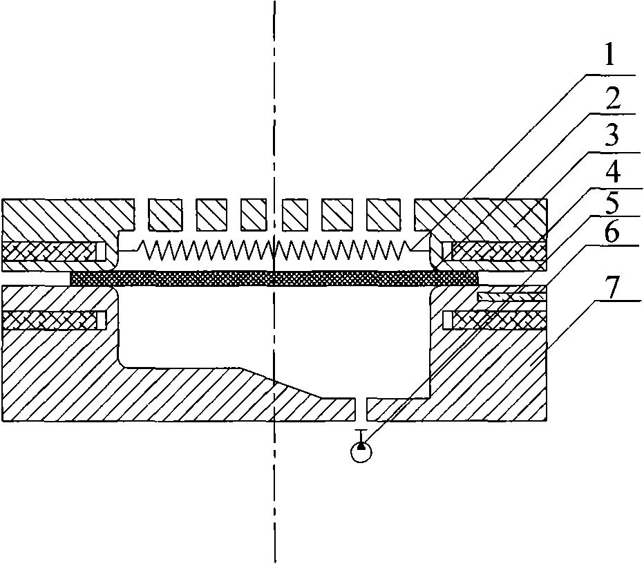
[0029] Combine below figure 1 and figure 2 This embodiment will be specifically described.
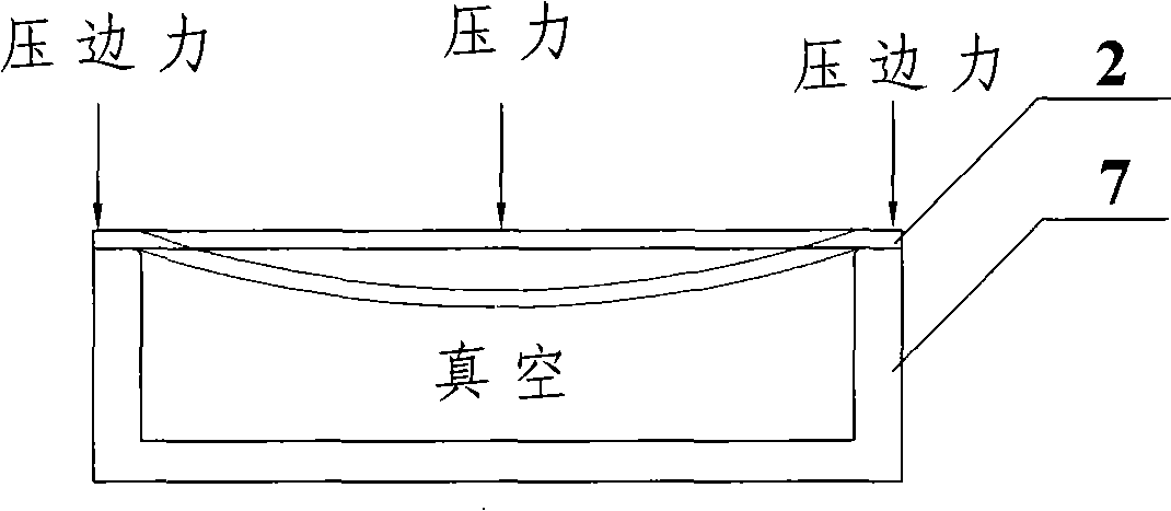
[0030] The processing device of the present invention is composed of a resistance wire 1 , a large amorphous alloy slab 2 , an upper plate 3 , an electric heating tube 4 , a vacuum pump 5 , a thermocouple 6 and a die 7 . Wherein: the large amorphous alloy slab 2 is placed between the upper pole plate 3 and the die 7, and is deformed under the joint action of the compressed air in the upper pole plate 3 and the vacuum in the inner cavity of the die 7. The upper pole plate 3 is assembled on the upper part of the large amorphous alloy slab 2. The upper pole plate 3 has a concave structure, and the top surface of the concave structure has air holes. The slabs 2 are crimped to form a compressed air chamber, and the upper plate is used for pressing the large amorphous alloy slab, heating and feeding compressed air to form the large amorphous alloy slab; the inner side of the concave struc...
Embodiment 2
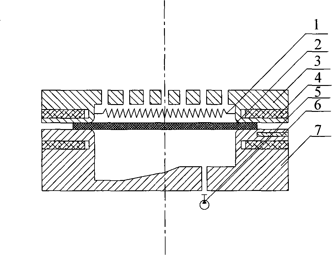
[0040] Combine below figure 1 and image 3 This embodiment will be specifically described.
[0041]The processing device of the present invention differs from Embodiment 1 in that: the die 7 has a hole at the key (button) position of the shell.
[0042] Processing technology of the present invention comprises the steps (see figure 1 ):
[0043] (1) According to the specific outline of the electronic product shell to be processed, design and process the upper plate 3 and the die 7, and select 110×70×0.7 (thick) mm Zr 65 al 10 Ni 10 Cu 15 Large amorphous alloy slab 2 . The large amorphous alloy slab 2 is placed in a heating furnace to start heating, and the heating temperature is between 400°C and 430°C (420°C is taken as an example in this embodiment).
[0044] (2) After the temperature in the heating furnace is stable, take out the large amorphous alloy slab 2 and place it on the top of the die 7 , and the die 7 is heated by the electric heating tube 4 . The upper pol...
PUM
 Abstract
Description
Claims
Application Information


