Optical close distance correction method, optical mask manufacture method and graphical method

An optical short-distance and manufacturing method technology, which is applied in the direction of optics, photographic process of pattern surface, and originals for photomechanical processing, etc., can solve the problems of semiconductor device failure and other problems, and achieve the effect of improving performance

Inactive Publication Date: 2008-11-26
SEMICON MFG INT (SHANGHAI) CORP
View PDF1 Cites 0 Cited by
  • Summary
  • Abstract
  • Description
  • Claims
  • Application Information

AI Technical Summary

Problems solved by technology

[0007] However, as the integration of semiconductor devices becomes higher, the critical dimensions of semiconductor devices become smaller and smaller. If the size of the line end part of the layout line pattern is increased, two reticle lines close to each other will be caused on the photomask. The pattern line ends are bridged, which in turn causes the two circuit pattern line ends on the wafer to also bridge, making the semiconductor device invalid

Method used


Image

  • Optical close distance correction method, optical mask manufacture method and graphical method
  • Optical close distance correction method, optical mask manufacture method and graphical method
  • Optical close distance correction method, optical mask manufacture method and graphical method

Examples


Embodiment Construction

[0023] The present invention forms a corresponding layout auxiliary pattern on opposite sides of the two line ends adjacent or opposite to the layout line pattern. The line ends of the reticle circuit pattern formed on the photomask and the line pattern formed on the wafer are inclined in opposite directions, so that no bridge is generated between the line ends, and the performance of the semiconductor device is improved.

[0024] The specific embodiments of the present invention will be described in detail below with reference to the accompanying drawings.

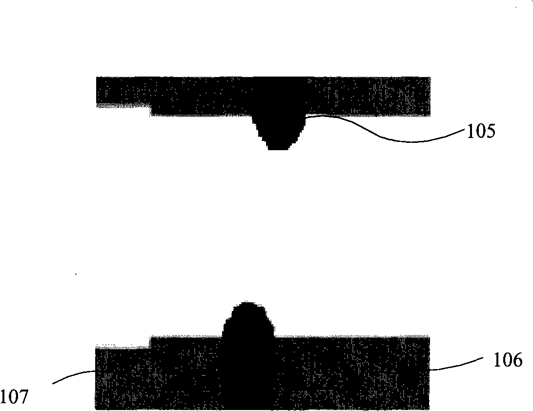
[0025] Figure 5 It is a flowchart of an embodiment of the present invention for optical close-range correction. Such as Figure 5 As shown, step S101 is performed to provide at least two adjacent or opposite layout line patterns; step S102 is performed to form corresponding layout auxiliary patterns on opposite sides of the two line ends.

[0026] Figure 6 It is a flowchart of an embodiment of the present invention for ma...


PUM


Abstract

An optical short-distance correction method comprises the procedures as follows: a layout circuit pattern is provided and the layout circuit pattern is provided with at least two close terminals; and layout auxiliary patterns are arranged oppositely to the two terminals respectively. The invention also provides a method for manufacturing a light masking template and a patterned method. As a result, at least two circuit pattern terminals formed on a wafer are prevented from bridging connection in between.

Description

Technical field [0001] The present invention relates to the technical field of semiconductor manufacturing, in particular to an optical proximity correction (OPC, Optical Proximity Correction) method, a photomask manufacturing method, and a patterning method. Background technique [0002] With the rapid development of semiconductor manufacturing technology, in order to achieve faster computing speed, larger data storage capacity and more functions, semiconductor chips are developing towards higher integration; and the higher the integration of semiconductor chips, Then the critical dimension (CD, Critical Dimension) of the semiconductor device is smaller. [0003] In order to realize a tiny CD, a finer image on the photomask must be focused on the photoresist of the semiconductor substrate, and the optical resolution must be enhanced to manufacture semiconductor devices close to the optical resolution limit in the photomask process. Resolution enhancement techniques include the u...

Claims


Application Information

Patent Timeline
Patent Type & Authority Applications(China)
IPC IPC(8): G03F1/14G03F1/36
Inventor 刘庆炜
Owner SEMICON MFG INT (SHANGHAI) CORP
Why Eureka
Try Eureka