Production of conducting wire

A manufacturing method and wire technology, applied in semiconductor/solid-state device manufacturing, electrical components, circuits, etc., can solve the problems of polysilicon layer 101 short circuit connection, side diffusion, polysilicon seepage, etc.

Active Publication Date: 2008-11-26
NEXCHIP SEMICON CO LTD
View PDF5 Cites 0 Cited by
  • Summary
  • Abstract
  • Description
  • Claims
  • Application Information

AI Technical Summary

Problems solved by technology

However, in the high-temperature annealing process, the polysilicon will seep out, causing lateral diffusion (Lateral Diffusion), resulting in the phenomenon that the metal silicide 106 is also formed on the insulating layer 102
When the distance between the two polysilicon layers 101 is very small and the metal silicide 106 is formed on the insulating layer 102 is very serious, a bridging phenomenon will be caused, resulting in the problem that the polysilicon layers 101 are short-circuited and connected together.

Method used


Image

  • Production of conducting wire
  • Production of conducting wire
  • Production of conducting wire

Examples


Embodiment Construction

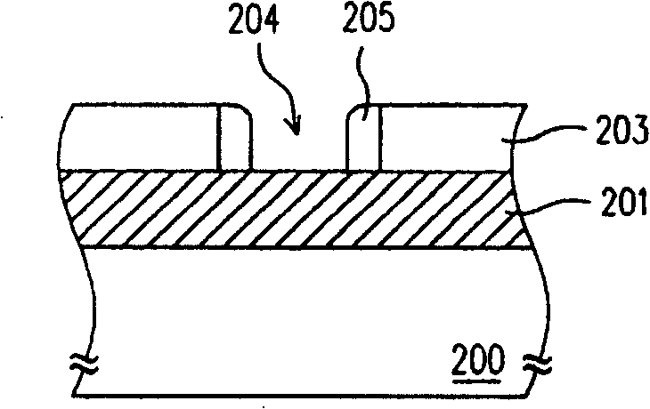
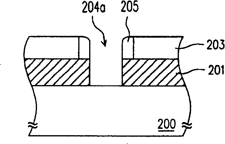
[0041] Figure 2A to Figure 2F is a cross-sectional view illustrating a manufacturing process of a wire according to a preferred embodiment of the present invention.

[0042] Please refer to Figure 2A In the method for manufacturing wires of the present invention, a substrate 200 is firstly provided, and a layer of polysilicon layer 201 has been formed on the substrate 200, and the formation method is, for example, chemical vapor deposition. Afterwards, a mask layer 203 is formed on the polysilicon layer 201 , which has an opening 204 exposing the polysilicon layer 201 . Wherein, the material of the mask layer 203 is, for example, silicon oxide or silicon nitride, and its formation method is, for example, to first form a mask material layer (not shown) by chemical vapor deposition, and then perform a photolithographic etching process to pattern the mask. mold material layer to form it.

[0043] Next, a spacer 205 is formed on the sidewall of the mask layer 203. The materia...


PUM


Abstract

The method comprises: providing a substrate on which a polycrystalline silicon layer has been already formed; forming a mask layer on the polycrystalline silicon layer; forming the spacer on the sidewall of the mask layer; using the mask layer having the spacer as the mask to remove a portion of polycrystalline silicon layer so as to expose the substrate; forming a insulating layer on the substrate filling out the opening, and the insulating layer and the mask layer has different etching selection; removing the mask layer to exposed the polycrystalline silicon layer; forming a metal silicides layer on the surface of the polycrystalline silicon layer.

Description

technical field [0001] The invention relates to a method for manufacturing a semiconductor element, in particular to a method for manufacturing a wire. Background technique [0002] As the integration of semiconductor components (Integrity) increases, the patterns and line widths in the corresponding components are also gradually reduced, resulting in an increase in the contact resistance between the gate and the wires in the component, resulting in a slower resistance-capacitance delay (RC Delay), This in turn affects the operating speed of the element. Since the resistance of metal silicide is lower than polysilicon (Polysilicon), and its thermal stability is also higher than that of general interconnection materials (such as aluminum), in order to reduce the contact resistance (Contact Resistance) when the wire is in contact with each electrode of the transistor, Metal silicide can be formed at the connection interface between each electrode of the transistor and the met...

Claims


Application Information

Patent Timeline
Patent Type & Authority Patents(China)
IPC IPC(8): H01L21/3205H01L21/768
Inventor 张骕远黄明山许汉杰
Owner NEXCHIP SEMICON CO LTD
Why Eureka
Try Eureka