Supercharge Your Innovation With Domain-Expert AI Agents!

Semiconductor device logic circuit

A logic circuit and semiconductor technology, applied in the field of logic circuits, can solve the problems of reduced space utilization and unreachable saturation current, and achieve the effects of reduced space, reduced hot-carrying ion effect, and high speed

Active Publication Date: 2008-11-26
SEMICON MFG INT (SHANGHAI) CORP
View PDF0 Cites 0 Cited by
  • Summary
  • Abstract
  • Description
  • Claims
  • Application Information

AI Technical Summary

Problems solved by technology

For traditional MOS semiconductor devices with ion depletion regions on three sides, the available space decreases rapidly, and the saturation current cannot reach the expected value when the applied voltage is reduced.

Method used


Image

  • Semiconductor device logic circuit
  • Semiconductor device logic circuit
  • Semiconductor device logic circuit

Examples


Embodiment Construction

[0029] In order to make the above objectives, features and advantages of the present invention more obvious and understandable, the specific embodiments of the present invention will be described in detail below with reference to the accompanying drawings.

[0030] In the following description, many specific details are explained in order to fully understand the present invention. However, the present invention can be implemented in many other ways different from those described herein, and those skilled in the art can make similar generalizations without violating the connotation of the present invention. Therefore, the present invention is not limited by the specific implementation disclosed below.

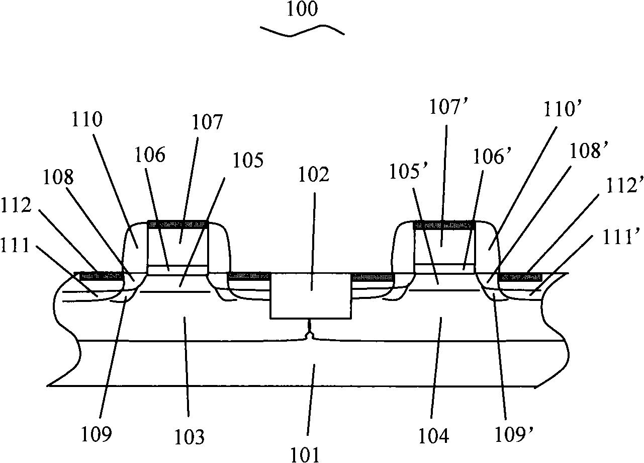
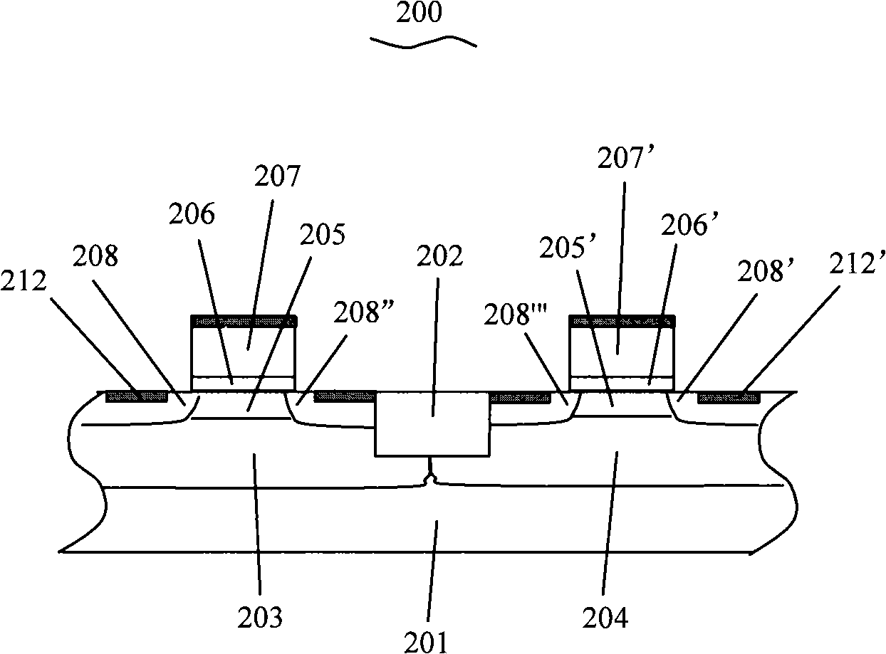
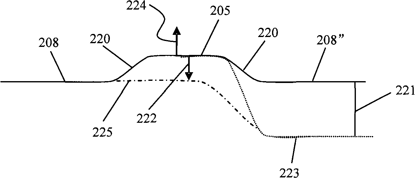
[0031] The essence of the present invention lies in the change of the basic principle of the structure of the semiconductor device, that is, the gate channel layer on the substrate and the source and drain on both sides of the charged ions are of the same type. The potential barrier...


PUM


Abstract

The invention discloses a logic circuit of a semiconductor device, in the structure of the semiconductor device, primary charged ions in a grid channel layer and in a source electrode and a drain electrode have the same forms. The grid channel layer can be separated from the source electrode and the drain electrode which are arranged on both sides of the grid channel layer without relying on PN junctions, the electric field effect of an external operation voltage can be more effectively utilized, the widely-ranged ion doping density and the dielectric layer thickness can be used. The required saturation current can be obtained while the voltage is reduced, which is adaptable to the production of smaller logic circuits of the semiconductor devices, with higher density.

Description

Technical field [0001] The present invention relates to the technical field of semiconductor integrated circuits, and in particular to a basic structure and operating principle of a metal oxide semiconductor (MOS) device and a logic circuit composed of it. Background technique [0002] In the MOS device structure in the logic circuit of a traditional semiconductor device, the dopants of the gate channel layer and the dopants of the source and drain on both sides are different types of charged ions. Please refer to Handbook of Semiconductor Manufacturing Technology. Edited by YoshioNishi and Robert Doering, publisher Marcel Dekker, Inc.in 2000. Chapter 5, by Robert B. Simonton, Walter Class, Yuri Erokhin, Michael Mack, and Leonard Rubin. figure 1 It is a schematic diagram of the structure of a prior art semiconductor device. Such as figure 1 In the semiconductor device 100 shown, an isolation shallow trench 102, a P-well 103 and an N-well 104 are sequentially formed on a semicon...

Claims


Application Information

Patent Timeline
Patent Type & Authority Applications(China)
IPC IPC(8): H01L27/092H01L29/78
Inventor 王津洲
Owner SEMICON MFG INT (SHANGHAI) CORP
Features
  • R&D
  • Intellectual Property
  • Life Sciences
  • Materials
  • Tech Scout
  • Unparalleled Data Quality
  • Higher Quality Content
  • 60% Fewer Hallucinations
Learn More