Design method for ultraviolet laser machining apparatus for cutting wafer

An ultraviolet laser and processing equipment technology, applied in laser welding equipment, metal processing equipment, welding equipment and other directions, can solve the problems of slow processing speed, cutting groove line width, high cost, high anti-vibration stability and positioning accuracy, high cutting The effect of yield

Active Publication Date: 2008-12-10
SUZHOU DELPHI LASER +1
View PDF0 Cites 64 Cited by
  • Summary
  • Abstract
  • Description
  • Claims
  • Application Information

AI Technical Summary

Problems solved by technology

Traditional wafer cutting is processed by mechanical methods such as grinding wheels and diamond knives. However, the mechanical processing method has the disadvantages of slow processing speed and wide cutting line. E

Method used


Image

  • Design method for ultraviolet laser machining apparatus for cutting wafer
  • Design method for ultraviolet laser machining apparatus for cutting wafer
  • Design method for ultraviolet laser machining apparatus for cutting wafer

Examples


Example Embodiment

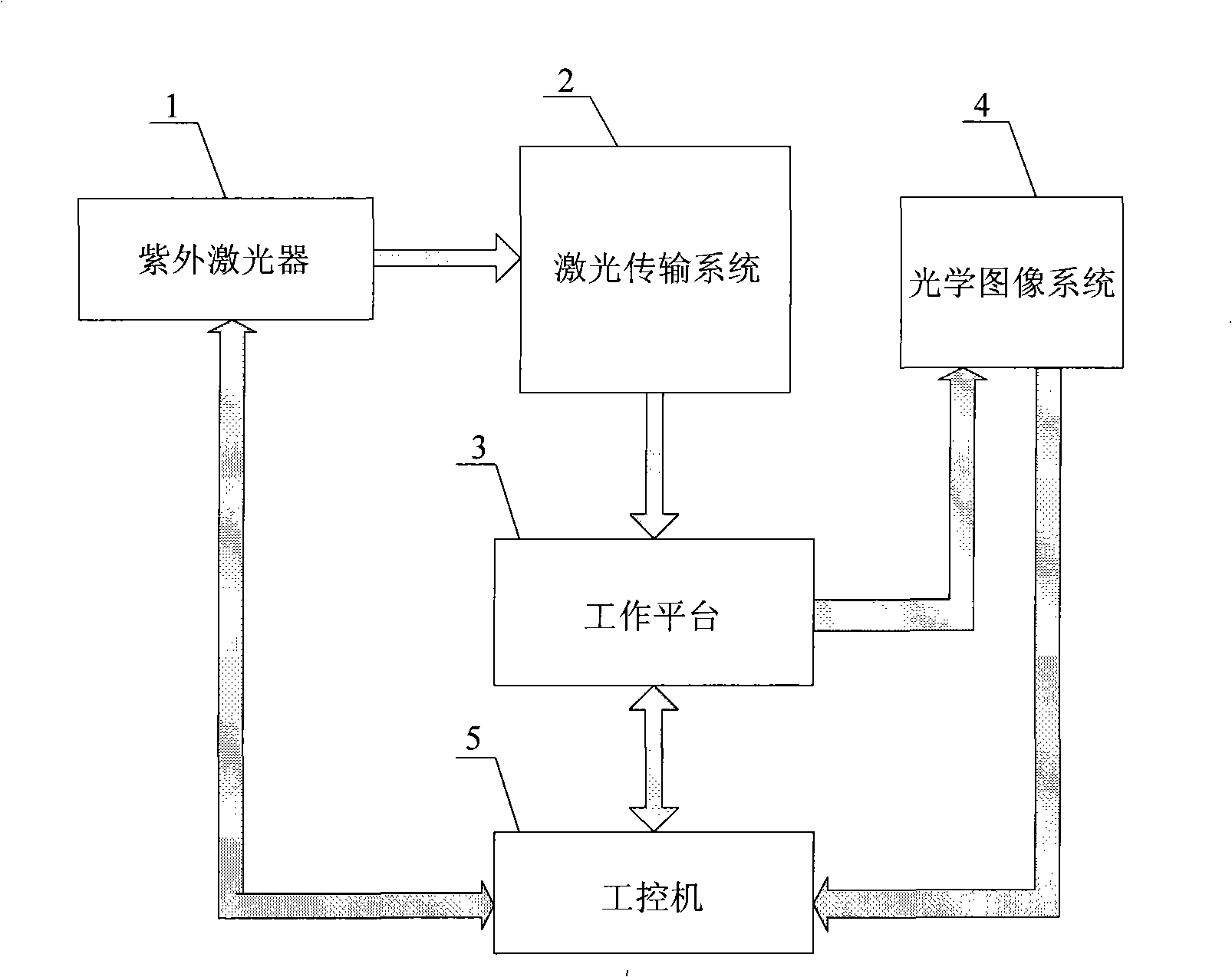
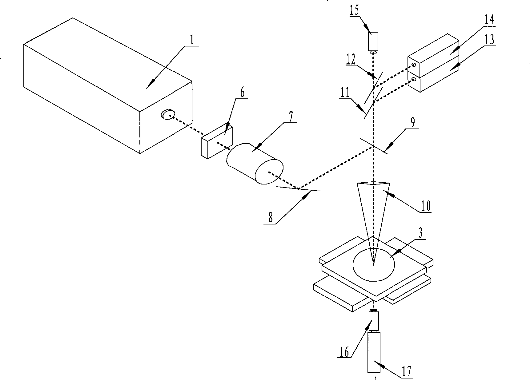
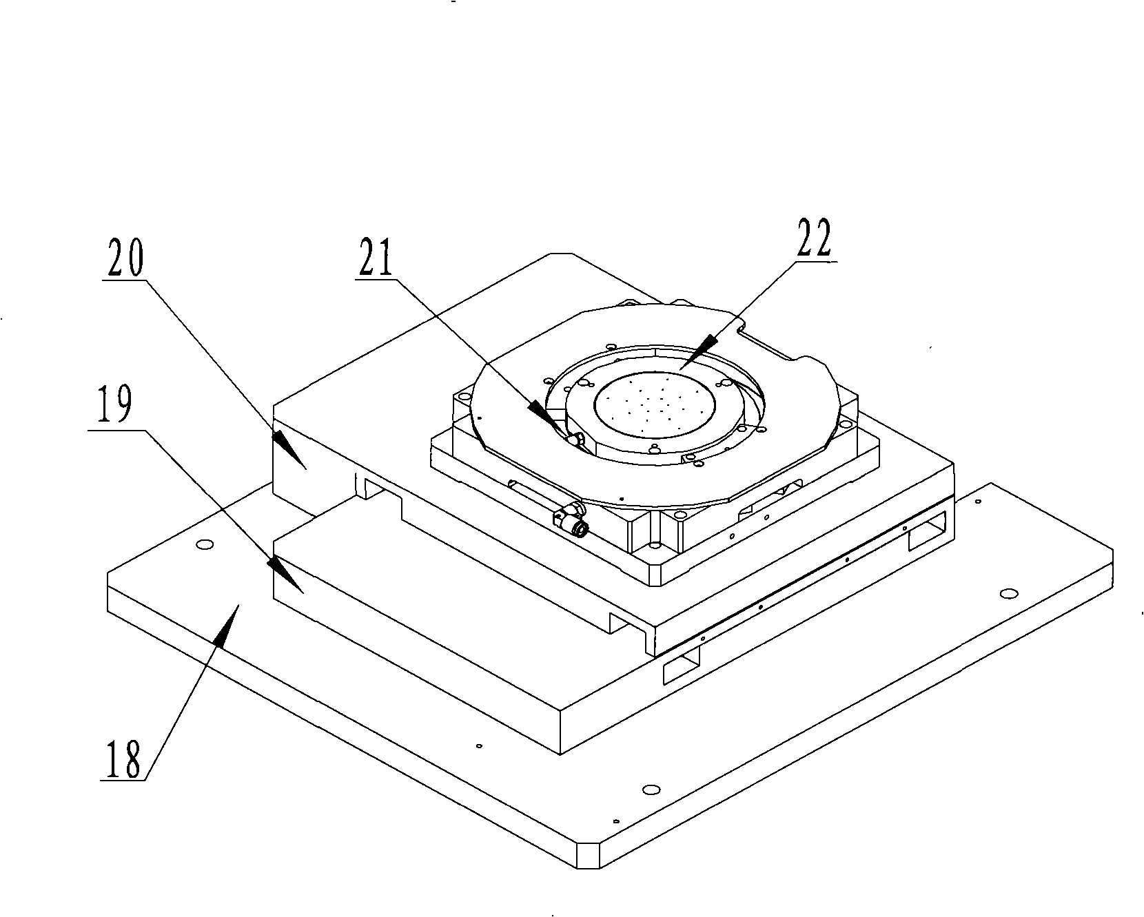
[0029] Such as figure 1 As shown, the wafer ultraviolet laser cutting equipment includes an ultraviolet laser 1, a laser transmission system 2, a processing platform 3, an optical image system 4, and an industrial computer 5. The ultraviolet laser 1 emits laser light and enters the laser transmission system 2. The laser transmission system 2 The high-energy-density focused spot is incident vertically on the processing platform 3, and the laser energy distribution focused on the surface of the processing platform is controlled by adjusting the optical components in the laser transmission system 2. The optical imaging system 4 is used to process the crystal before laser cutting. The circle is used for positioning and cutting trajectory planning. During laser cutting, the laser optical axis remains stationary while the processing platform 3 moves linearly in the X and Y axes relative to the optical axis; the ultraviolet laser 1 communicates with the industrial computer 5 through the...


PUM


Abstract

The invention relates to a design method for ultraviolet laser processing equipment used in the wafer cutting; lasers emitted by an ultraviolet laser are injected to a laser transmission system which can vertically inject focus spots with high energy density to a processing platform; the laser energy distribution focused on the surface of the processing platform is controlled by adjusting optical components in the laser transmission system; the wafer that is about to be processed is positioned and the cutting tracks are planned by an optical image system before the laser cutting; a laser optical axis keeps still and the processing platform carries out the linear motions along an X axis and a Y axis during the laser processing; an industrial computer conveys control instructions to the laser while the laser conveys state information to the industrial computer, and the optical image system transmits the taken image information of the work piece surface to the industrial computer to carry out the image processing. The design method adopts an optical path design with simple and complete functions, controls the spot energy distribution of the laser processing platform conveniently and flexibly and can be applied to the semi-conductor wafer sheet cutting of a plurality of materials and specifications.

Description

technical field [0001] The invention relates to a laser cutting device, in particular to a design method of an ultraviolet laser high-precision processing device used for semiconductor wafer cutting. Background technique [0002] Semiconductor wafers are often grown on substrate materials with similar crystal lattices by vapor deposition. Before semiconductor devices are packaged in terminal applications, wafers of several inches need to be cut into smaller sized grains. Traditional wafer cutting is processed by mechanical methods such as grinding wheels and diamond knives. However, the mechanical processing method has the disadvantages of slow processing speed and wide cutting line. Especially when cutting hard substrates like sapphire, the mechanical cutting efficiency is low. The cost is high. Cutting a 2-inch wafer is generally 1 to 2 pieces per hour, and each diamond blade can only cut 2 to 3 pieces. [0003] With the development of the semiconductor industry, there ar...

Claims


Application Information

Patent Timeline
IPC IPC(8): B23K26/38B23K26/40B23K26/04B23K26/08G02B27/00H01L21/78B23K26/402
Inventor 赵裕兴徐海宾
Owner SUZHOU DELPHI LASER
Why Eureka
Try Eureka