Encapsulation of silicon substrate LED

An encapsulation method and technology of silicon substrate, which are applied to electrical components, circuits, semiconductor devices, etc., can solve the problems of reducing the transparency of epoxy resin and increasing the cost, and achieve the effects of low cost, low defective rate and optimized operation mode.

Active Publication Date: 2008-12-10
JIANGXI LATTICEBRIGHT
View PDF1 Cites 13 Cited by
  • Summary
  • Abstract
  • Description
  • Claims
  • Application Information

AI Technical Summary

Problems solved by technology

The disadvantage of this is to increase the cost and reduce the transparency of the epoxy resin

Method used


Image

  • Encapsulation of silicon substrate LED
  • Encapsulation of silicon substrate LED

Examples


Embodiment Construction

[0022] The invention provides a silicon substrate LED packaging method.

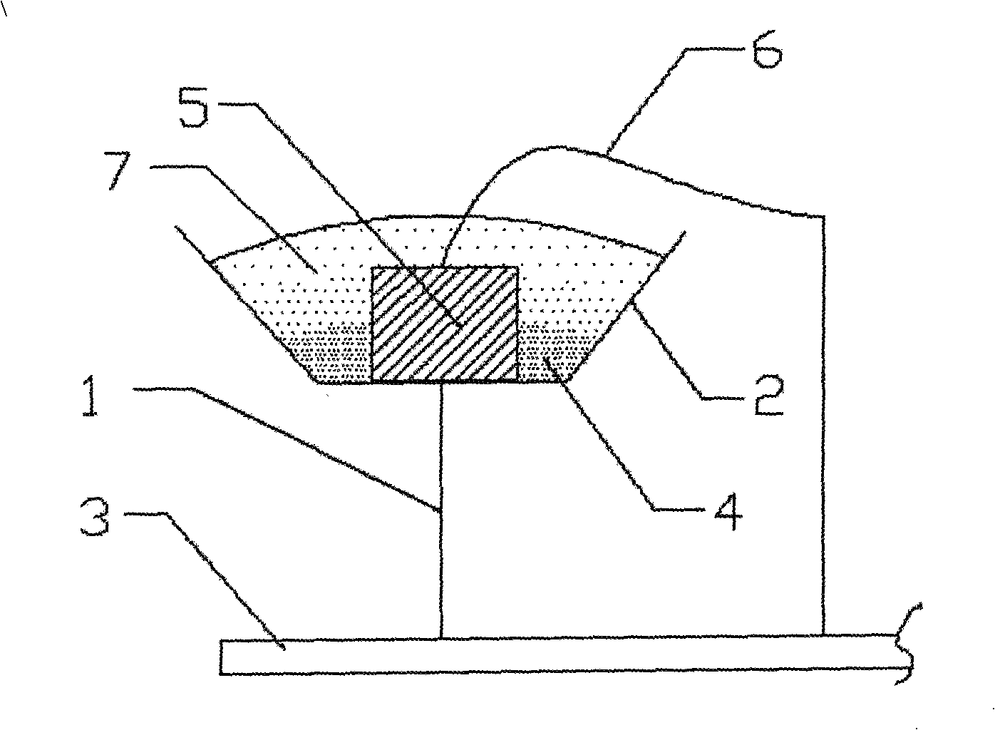
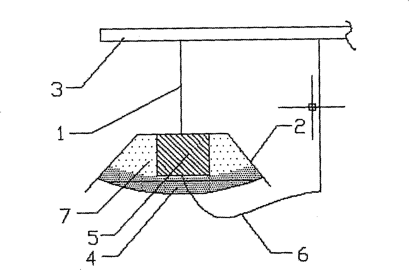
[0023] The embodiments of the present invention take an LED chip made of gallium nitride material as an example. Gallium nitride is the luminescent material for blue and green LED chips, and an 8mil blue chip is used to produce white light, and the height of the chip containing the silicon substrate is 200 μm. The chip electrode is a single electrode structure.

[0024] Test one, see figure 1 , made according to traditional techniques:

[0025] Wire bonding, solder wire 6, connect the electrode of the chip 5 to the pin of the bracket 1; mix the glue, mix the phosphor powder 4 in the transparent epoxy resin 7; dispense glue, fill the epoxy resin mixture into the reflector 2 In the process, the chip 5 is covered to form a lens shape that is conducive to astigmatism; for curing, the LEDs that have been glued are placed in a curing furnace for baking and curing. The curing temperature is 130 degrees Celsi...


PUM


Abstract

The invention discloses a packaging method for a silicon substrate LED. The method comprises: pointing glue, packing the LED chip in the reflective cup with the transparent colloid mixed with the fluorescent powder; baking and solidifying: placing the LED chip with the glue in the solidifying oven for the solidifying and molding; while processing the solidifying, firstly reversely placing the LED chip with the glue, and then placing the chip in the solidifying oven for the solidifying and molding. The method is used for solidifying the fluorescent powder at the upper position of the lighting chip to sufficiently use the fluorescent powder to obtain a great effect of white light for the LED lamp under the situation of not increasing the fluorescent powder on the silicon substrate LED chip. The invention is suitable for the thick LED chip with the silicon substrate, which has the advantages of lower cost, greater effect, simpler procedure, and lower defective rate.

Description

technical field [0001] The invention relates to a silicon substrate LED, in particular to its packaging method. Background technique [0002] The LED packaging method in the prior art is described in the background technology of the patent document with the Chinese patent application number 200620040942.2 and the title "High Brightness and High Reliability Sapphire Substrate-Based Light Emitting Diode". [0003] The packaging method of LED is briefly described as: wire bonding, soldering wires, connecting the chip electrodes to the bracket pins; mixing glue, mixing phosphor powder into transparent epoxy resin; dispensing glue, filling the epoxy resin mixture into the reflective cup In the process, the chip is covered to form a lens shape that is conducive to astigmatism; for curing, the LEDs that have been glued are placed in a curing oven for baking and curing; then the ribs are punched, and the cured LED lights are cut from the base of the bracket ; Test, test screening a...

Claims


Application Information

Patent Timeline
Patent Type & Authority Applications(China)
IPC IPC(8): H01L33/00
Inventor 曾平
Owner JIANGXI LATTICEBRIGHT
Why Eureka
Try Eureka