High on-stage voltage right-handed LED integrated chip and manufacturing method thereof
A technology of integrated chips and manufacturing methods, applied in semiconductor/solid-state device manufacturing, circuits, electrical components, etc., can solve the problems of poor high-voltage resistance performance of LED integrated chips, and achieve a small footprint, small chip integration, and cost reduction. Effect
- Summary
- Abstract
- Description
- Claims
- Application Information
AI Technical Summary
Problems solved by technology
Method used
Image
Examples
Embodiment 1
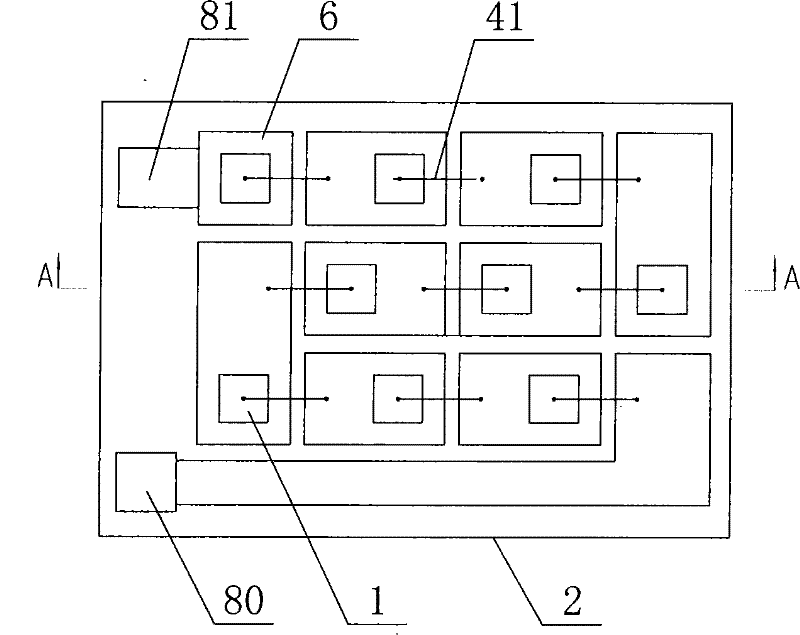
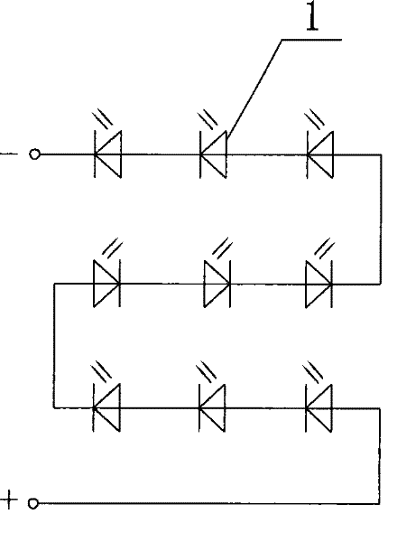
[0045] like figure 1 , image 3 , Figure 4 As shown, the high conduction voltage front-mounted LED integrated chip of this embodiment includes nine LED bare chips 1 and a silicon substrate 2, the LED bare chips 1 are single-electrode chips, and the LED bare chips 1 include gallium arsenide ( GaAs) substrate 10 and N-type epitaxial layer 11, P-type epitaxial layer 12, certainly, described substrate 10 also can be the substrate of other materials such as silicon carbide (SiC), described silicon substrate 2 is P-type silicon substrate, the front side of the silicon substrate 2 is formed with a thermally conductive insulating layer, and the thermally conductive insulating layer is solely composed of a second thermally conductive insulating layer 5 formed by deposition, and the second thermally conductive insulating layer 5 is composed of a silicon nitride layer, The thermal conductivity of silicon nitride is very high, and its thermal conductivity is more than 100 times higher ...
Embodiment 2
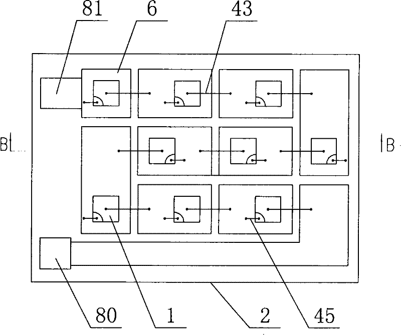
[0054] like figure 2 , image 3 , Figure 5 to Figure 9 As shown, the difference between this embodiment and Embodiment 1 is that: the LED bare chip 1 is a double-electrode chip, and the substrate 10 is aluminum oxide (sapphire, Al 2 O 3 ) substrate, the P-type epitaxial layer 12 and the N-type epitaxial layer 11 are soldered to two adjacent metal layers 6 through metal wires 43 and 45 respectively.
[0055] The remaining features of this embodiment are the same as those of Embodiment 1.
Embodiment 3
[0057] like figure 1 , image 3 , Figure 10 As shown, the difference between the high turn-on voltage front-mounted LED integrated chip of this embodiment and the first embodiment is that a layer of N+ diffusion layer 3 is diffused inwardly from the front side of the silicon substrate 2 described in this embodiment, and the N+ A first thermally conductive insulating layer 4 is grown on the diffusion layer 3, a second thermally conductive insulating layer 5 is deposited on the first thermally conductive insulating layer 4, and a metal layer 6 is deposited on the second thermally conductive insulating layer 5, that is, the The thermally conductive insulating layer is composed of the first thermally conductive insulating layer 4 formed by growth and the second thermally conductive insulating layer 5 formed by deposition, the first thermally conductive insulating layer 4 is made of silicon dioxide, and the second thermally conductive insulating layer 5 is composed of silicon ni...
PUM
 Abstract
Description
Claims
Application Information
 - R&D
- Intellectual Property
- Life Sciences
- Materials
- Tech Scout
- Unparalleled Data Quality
- Higher Quality Content
- 60% Fewer Hallucinations
Browse by: Latest US Patents, China's latest patents, Technical Efficacy Thesaurus, Application Domain, Technology Topic, Popular Technical Reports.
© 2025 PatSnap. All rights reserved.Legal|Privacy policy|Modern Slavery Act Transparency Statement|Sitemap|About US| Contact US: help@patsnap.com


