Insulated gate transistor incorporating diode and inverter circuit

An insulated gate type, transistor technology, applied in circuits, semiconductor devices, electrical components, etc., can solve the problems of small effect, deterioration of reverse leakage current and reverse withstand voltage characteristics, and small improvement effect of recovery characteristics, etc.

Active Publication Date: 2008-12-24
MITSUBISHI ELECTRIC CORP
View PDF8 Cites 7 Cited by
  • Summary
  • Abstract
  • Description
  • Claims
  • Application Information

AI Technical Summary

Problems solved by technology

Therefore, it can be considered that the effect of forming a P-layer in the P-layer of the surface is small
In particular, since hole injection from a high-concentration base layer is dominant in recovery characteristics at high current, it is considered that the improvement effect on recovery characteristics at high current is small in the above-mentioned proposal of the publication.
However, if this area is simply enlarged, the reverse leakage current and reverse withstand voltage characteristics will deteriorate.
Therefore, it is difficult to say that the above-mentioned proposal in this gazette is an effective proposal for improving the recovery characteristics of the built-in FWD.
[0024] In addition, although the problem of "improvement of the recovery characteristics of the built-in diode" occurs particularly remarkably in the IGBT with a built-in FWD, it can be said that such a problem also occurs in a vertical MOSFET (power MOSFET) with a built-in FWD. technical issues

Method used


Image

  • Insulated gate transistor incorporating diode and inverter circuit
  • Insulated gate transistor incorporating diode and inverter circuit
  • Insulated gate transistor incorporating diode and inverter circuit

Examples


Embodiment Construction

[0106] In the following, cases where the subject matter of the present invention is applied to a trench gate type IGBT device will be described, but it should be noted that the idea of ​​each technology that is clear from the description of each embodiment described below will be described later. Basically, vertical MOSFETs with a trench gate structure are also applicable.

[0107] (Embodiment 1)

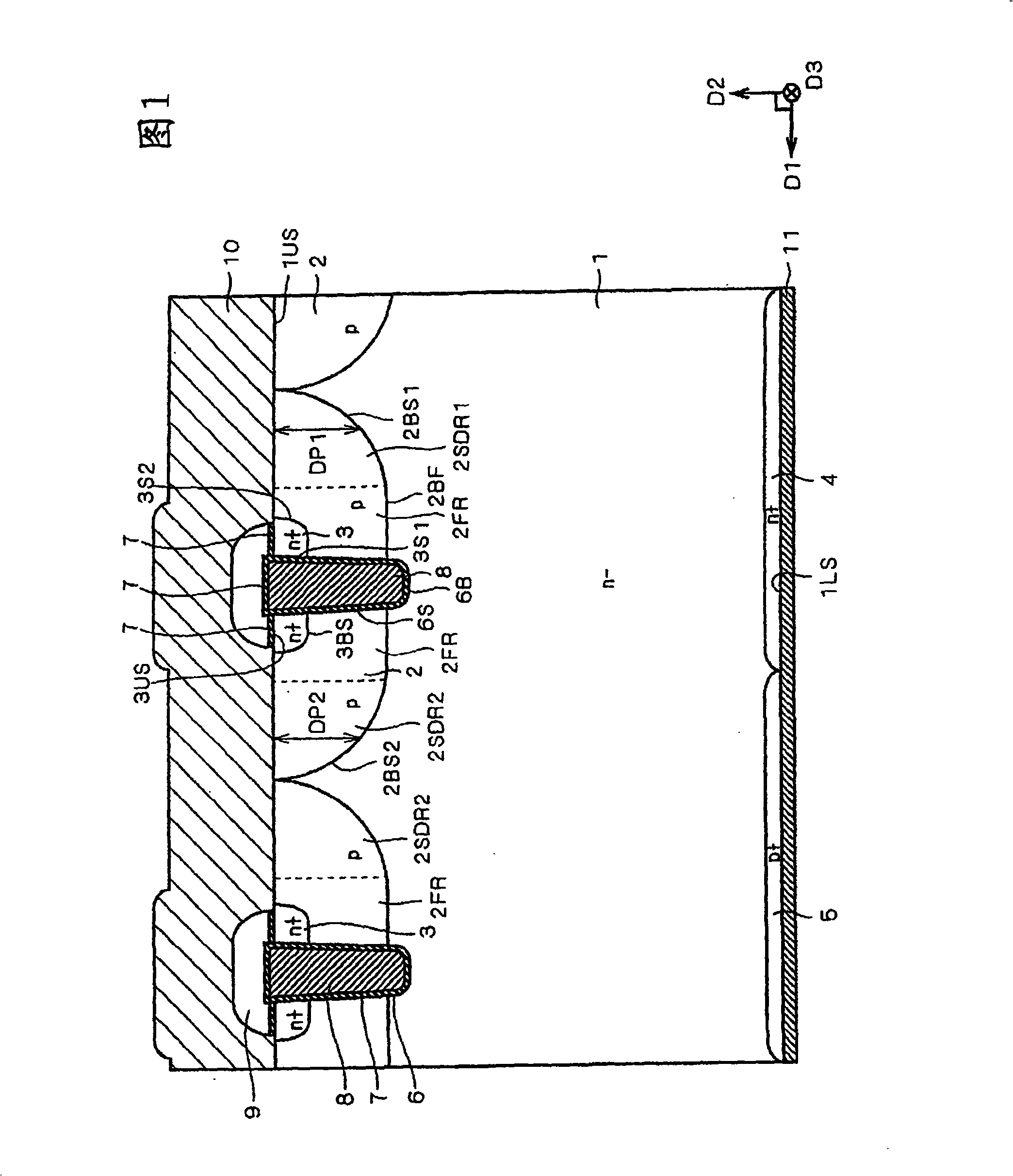
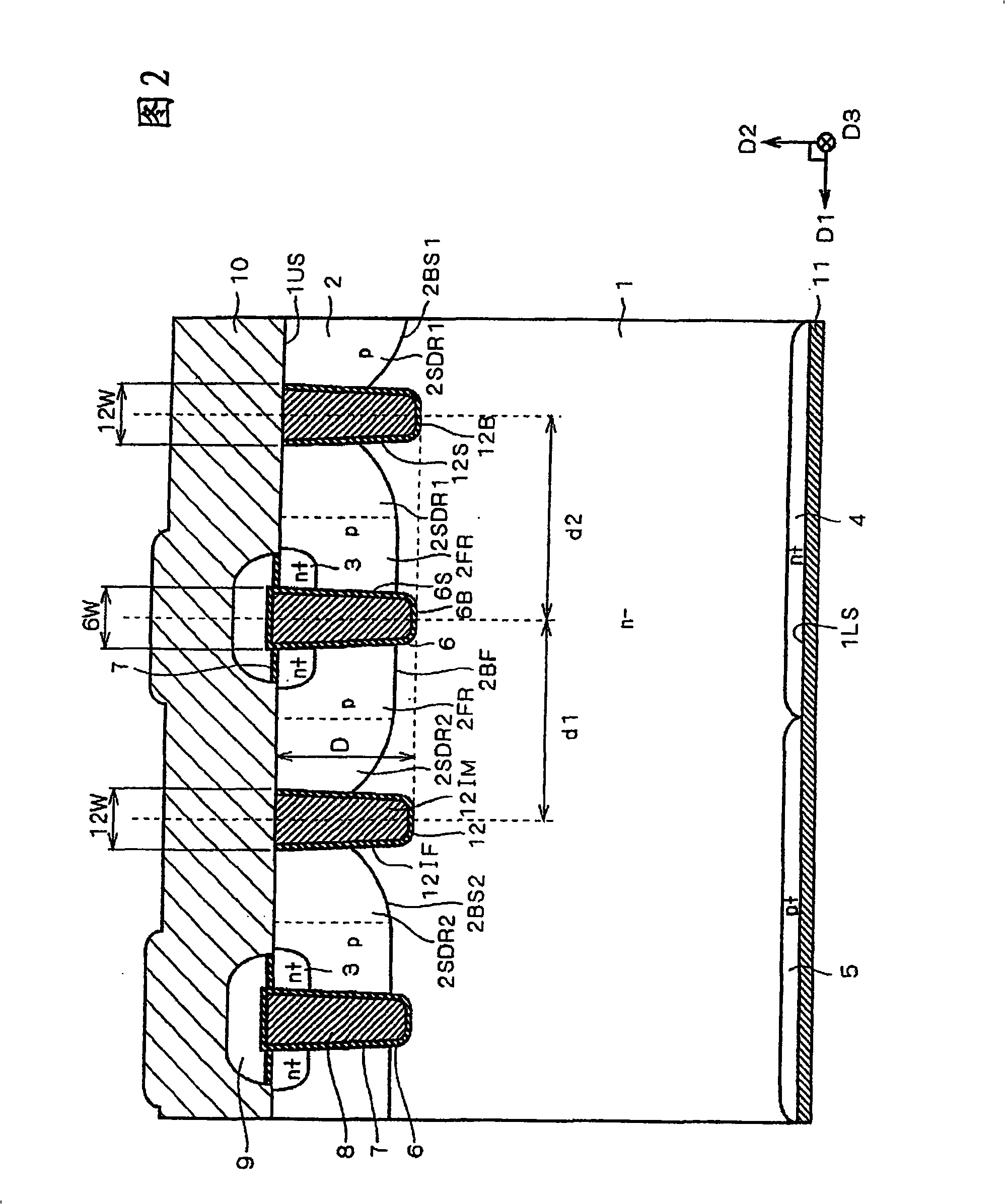
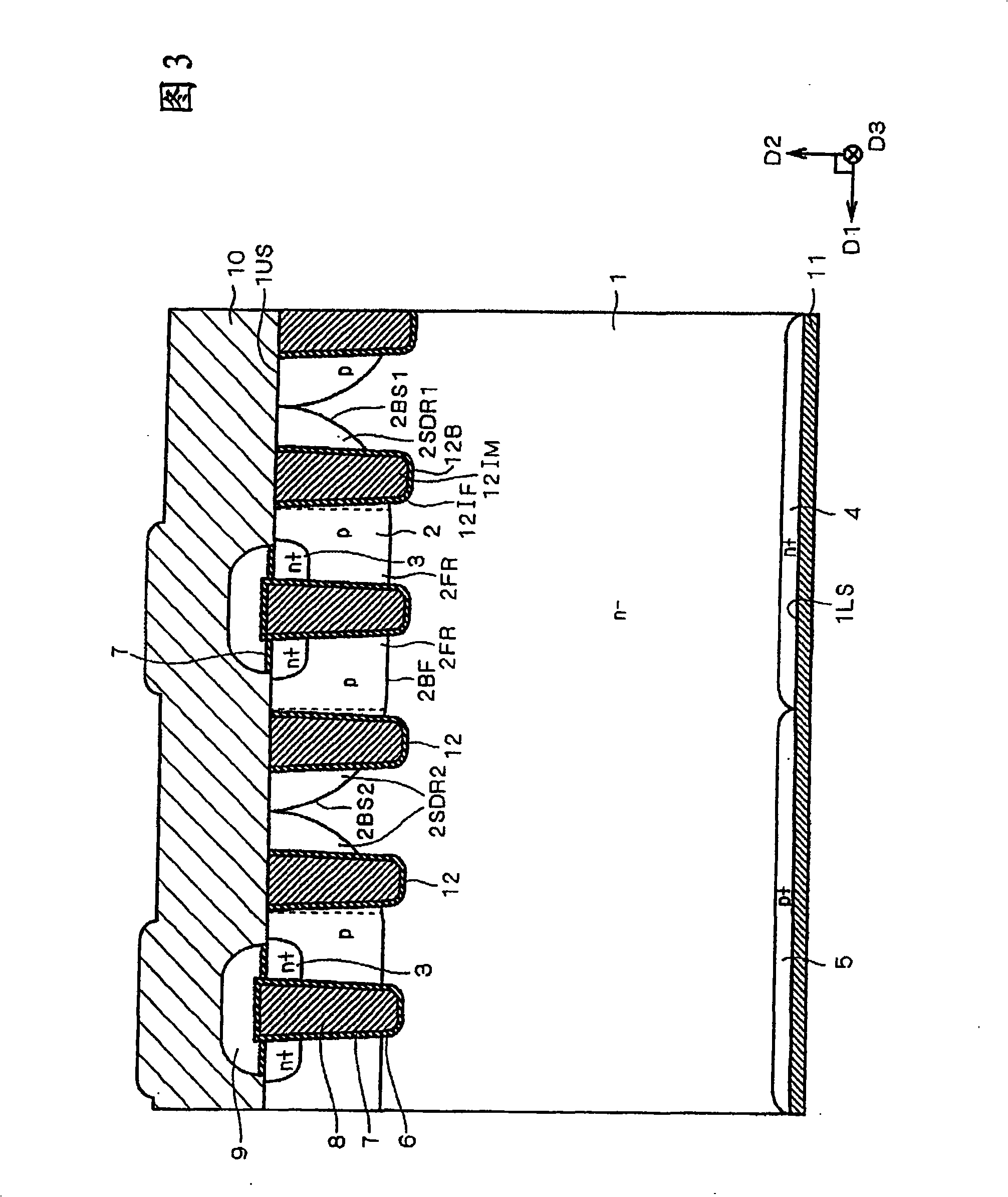
[0108] The characteristic points and core parts of the IGBT cell (IGBT unit cell + built-in diode cell) of the trench gate IGBT device of this embodiment are as understood with reference to the longitudinal sectional view 1 described later. The first main surface 1US of the semiconductor substrate 1 (here, N-type as an example) is formed in a well shape toward the inside of the semiconductor substrate 1 and has a flat surface whose bottom surface 2BF is formed substantially parallel to the first main surface 1US. The second conductivity type of the flat region 2FR, the first side d...


PUM


Abstract

The invention provides an insulated gate bipolar transistor and an inverter circuit and improves the recovery characteristic of diode action in a FWD built-in type nsulated gate bipolar transistor. A p-type base layer shaped like a well is formed for each of IGBT cells, and a p<+>-type collector layer (5)and an n<+>-type cathode layer(4) are formed on a surface opposite to a surface on which the p-type base layer is formed so as to be situated just below the p-type base layer. The p-type base layer (2) of each of the IGBT cells includes a flat region including an emitter region and a bottom surface penetrated by a main trench (6), and first and second side diffusion regions between which the flat region is interposed. The first side diffusion region is situated just above the n<+>-type cathode layer (4)and each of the bottom surfaces of the side diffusion regions forms a parabola-shaped smooth curve in longitudinal section. By replacing the p<+>-type collector layer (5) with the n<+>-type cathode layer (4), it is possible to apply features of the above structure to a power MOSFET.

Description

[0001] This application is a divisional application of a Chinese patent application filed on August 26, 2004 with application number 200410064437.8 and the title of the invention is "Insulated Gate Transistor and Inverter Circuit". technical field [0002] The present invention relates to a transistor having an insulated gate (MOS structure) (for example, an insulated gate bipolar transistor (hereinafter also referred to as an IGBT. In addition, such an IGBT is also referred to as a reverse conduction IGBT.) or a power MOSFET, etc.), In particular, it relates to the structure of an insulated gate transistor having a trench gate structure in which a diode unit functioning as a freewheeling diode (hereinafter also simply referred to as FWD) is mounted and its manufacturing technology. Furthermore, the present invention is a technique for improving recovery characteristics during diode operation of a diode cell mounted in an insulated gate transistor. Background technique [00...

Claims


Application Information

Patent Timeline
Patent Type & Authority Applications(China)
IPC IPC(8): H01L29/739H01L29/78H01L29/06H01L29/40
Inventor 高桥英树
Owner MITSUBISHI ELECTRIC CORP
Why Eureka
Try Eureka