Multilayer printed wiring plate, and method for fabricating the same

A multi-layer printing and circuit board technology, which is applied in the fields of printed circuit manufacturing, multi-layer circuit manufacturing, printed circuit, etc., can solve problems such as misoperation and misidentification

Inactive Publication Date: 2012-06-27
IBIDEN CO LTD
View PDF2 Cites 0 Cited by
  • Summary
  • Abstract
  • Description
  • Claims
  • Application Information

AI Technical Summary

Problems solved by technology

[0005] As an example of such a problem, when an off signal appears, it may be misrecognized as an on signal due to external noise, which may cause malfunction, etc.
In addition, in semiconductor devices, there may be cases where an off signal is mistakenly recognized as an on signal due to the influence of noise, and as a result, it may be affected by malfunctions, etc.

Method used


Image

  • Multilayer printed wiring plate, and method for fabricating the same
  • Multilayer printed wiring plate, and method for fabricating the same
  • Multilayer printed wiring plate, and method for fabricating the same

Examples


Embodiment 1-1

[0224] (1) Prepare the substrate

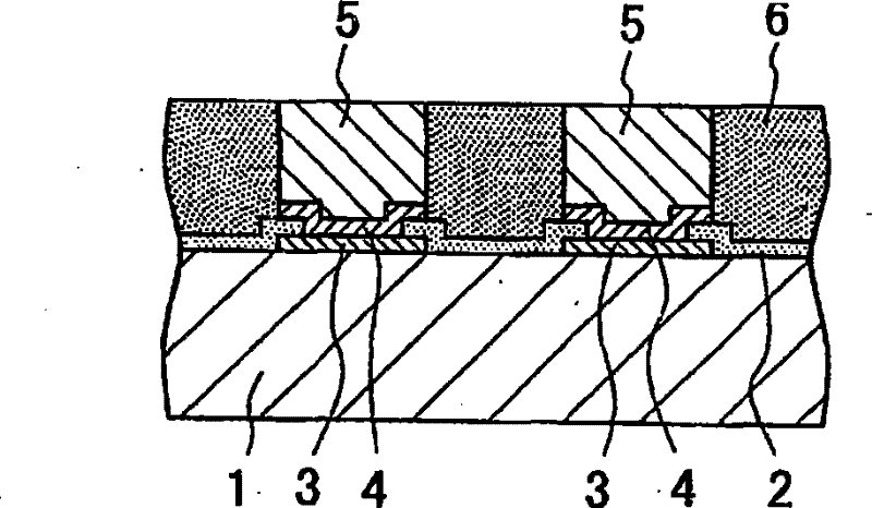
[0225] First, a printed circuit board constituting a substrate for accommodating a semiconductor element is produced. This printed circuit board is formed by the 1st insulating base material 30 and the 2nd insulating base material 40, and these base materials are laminated|stacked to form this printed circuit board. As an example of the material of the printed circuit board, a double-sided copper-clad laminate obtained by laminating prepreg cloth and copper foil and heating and pressing is used as a starting material. Cloth is made by impregnating epoxy resin into glass cloth to make B-stage.

[0226] As the first insulating base material 30, a double-sided copper-clad laminate in which copper foil 34 with a thickness of 15 μm is attached to both surfaces of a resin insulating layer 32 with a thickness of 60 μm was used. . The copper foil 34 of this laminated board can use the copper foil thicker than 15 μm, by etching, the thickness of th...

Embodiment 1-2

[0356] Except for embedding the semiconductor element 55 having an intermediate layer produced by the following steps (a) to (c) into the concave portion 42 of the substrate for accommodating the semiconductor element, the same process as in Example 1-1 was carried out to manufacture a multilayer printed circuit. plate.

[0357] (a) Continuously form a two-layer film of a chromium thin film and a copper thin film layer on the chromium thin film in a vacuum chamber by sputtering on the entire surface of the semiconductor element, and the semiconductor element is formed with a protective film on the connection pad and the wiring pattern. film, the thickness of the chromium thin film is 0.1 μm, and the thickness of the copper thin film layer is 0.5 μm.

[0358] (b) Next, a plating resist layer using a dry film is formed on the thin film layer. A mask on which a portion for forming an intermediate layer was drawn was mounted on the plating resist layer, and exposed and developed ...

Embodiment 1-3

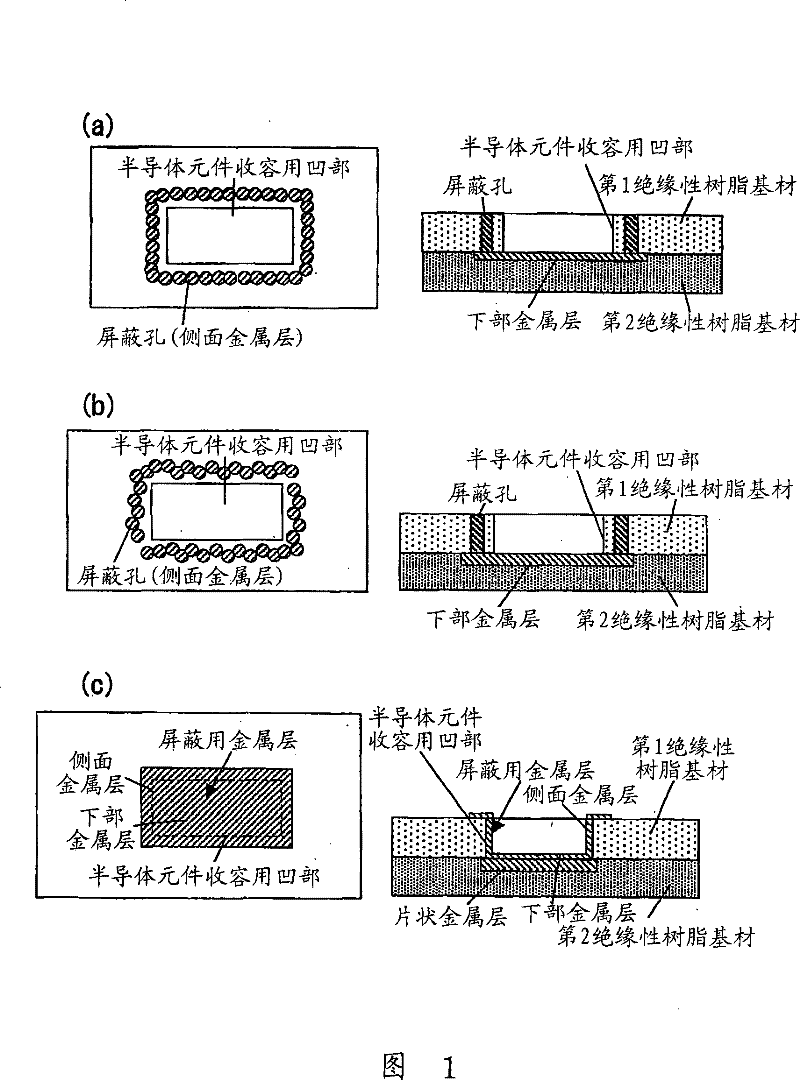
[0362] In addition to forming the shielding hole as figure 1 Except for the zigzag arrangement (staggered arrangement) as shown in (c), the same process as in Example 1-1 was performed to manufacture a multilayer printed wiring board.


PUM

PropertyMeasurementUnit
thicknessaaaaaaaaaa
thicknessaaaaaaaaaa
diameteraaaaaaaaaa

Abstract

Provided is a multilayer printed wiring plate, in which an insulating resin film and conductor circuits are formed over another insulating resin layer housing a semiconductor element and in which the conductor circuits are electrically connected with each other through a via hole, wherein an electromagnetic shield layer is formed either in the insulating resin layer enclosing a recess for housingthe semiconductor element or in the inner wall face of the recess, and wherein the semiconductor element is mounted in the recess.

Description

technical field [0001] The present invention relates to multilayer printed wiring boards incorporating electronic components (semiconductor elements) such as ICs. More specifically, it relates to methods for ensuring electrical connectivity and connection reliability between pads of semiconductor elements and conductor circuits of multilayer printed wiring boards. Multilayer printed circuit board and its manufacturing method. Background technique [0002] As a multilayer printed wiring board incorporating a semiconductor element, for example, there is a multilayer printed wiring board disclosed in JP-A-2001-339165 or JP-A-2002-050874. The multilayer printed wiring board disclosed in these documents is composed of a substrate, a semiconductor element, an insulating layer, a conductor circuit, and a via hole, the substrate is formed with a recess for embedding the semiconductor element, and the semiconductor element is embedded in the recess of the substrate, The insulating l...

Claims


Application Information

Patent Timeline
Patent Type & Authority Patents(China)
IPC IPC(8): H05K3/46
CPCH01L2924/01015H01L2924/01023H01L2924/01046H01L2924/15153H01L2224/2402H01L2924/01082H01L2924/01045H01L2924/15157H01L23/552H01L2924/3511H01L2924/01002H01L2924/1517H05K2203/0733H01L2924/01019H01L24/82H01L2924/01029H05K1/185H01L23/49822H01L2924/01027H01L24/24H01L2924/014H01L2924/01013H01L2924/01024H05K3/4652H01L2924/0103H01L2224/82039H05K1/0218H01L2924/15331H01L2924/01047H01L2924/01079H01L2924/14H05K2201/09981H01L2924/01005H01L2924/01033H01L2924/01006H05K1/183H01L2924/01074H01L2924/01078H01L2924/01011H01L2924/01012H01L2924/3025H01L23/5389H01L2924/15788H01L2924/12042H01L2224/04105H01L2224/12105H01L2224/73267Y10T29/49155H01L2924/00H05K3/46H05K1/18
Inventor 伊藤宗太郎高桥通昌三门幸信
Owner IBIDEN CO LTD
Why Eureka
Try Eureka