Microlens array of curved surface and preparation method thereof
A microlens array and microlens technology, applied in other household appliances, coupling of optical waveguides, optical elements, etc., can solve problems such as the difficulty of directly applying microlens arrays, achieve simple, reliable and feasible process, low cost, and reliable structure control effect
- Summary
- Abstract
- Description
- Claims
- Application Information
AI Technical Summary
Problems solved by technology
Method used
Image
Examples
Embodiment 1
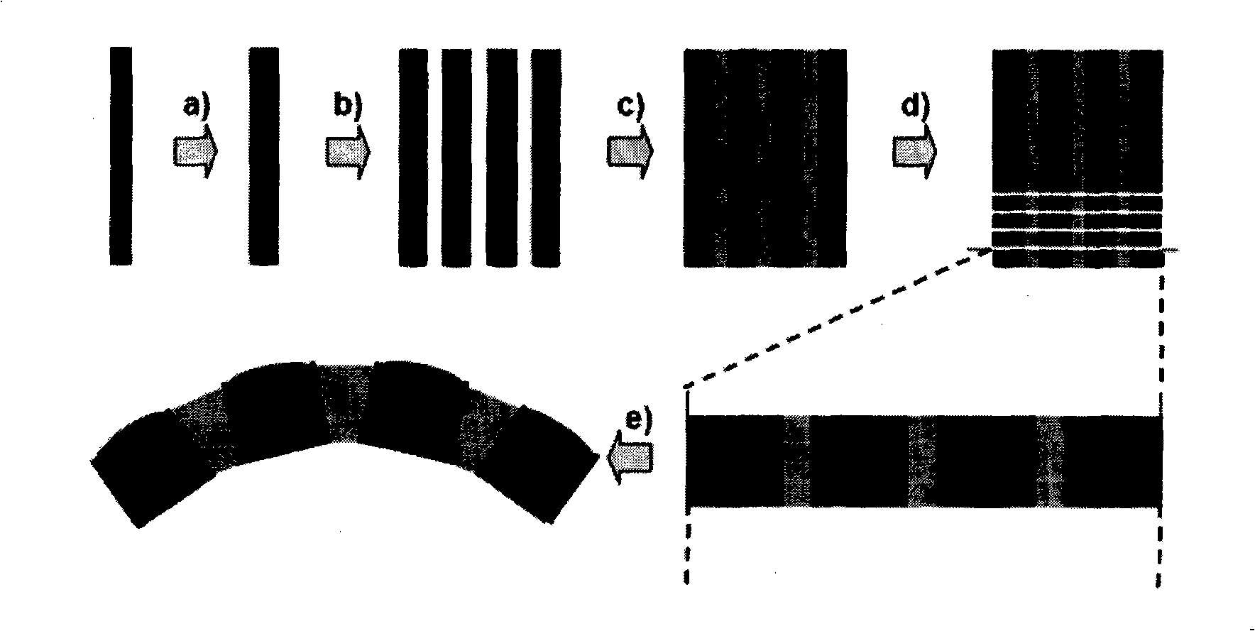
[0016] Embodiment 1: the polymethyl methacrylate (PMMA) fiber surface that is 1000 μ m in diameter is coated with a layer of nickel metal layer with a thickness of 100 μ m by electroplating, then after it is assembled into an ordered structure, it is filled with PMMA by melting method to form metal - Polymer composite structure, cut into 1000 μm slices along the direction perpendicular to the fiber axis, place it on a curved substrate and heat it to 150°C to form a microlens array with a curved surface.
Embodiment 2
[0017] Example 2: The surface of a polystyrene (PS) fiber with a diameter of 250 μm is coated with a copper metal layer with a thickness of 5 μm by electroless plating, and then it is assembled into an ordered structure and filled with polystyrene (PS) by polymerization. ) to form a metal-polymer composite structure, cut into 200 μm thin slices along the direction perpendicular to the fiber axis, place it on a curved substrate and heat it to 150°C to form a microlens array with a curved surface.
Embodiment 3
[0018] Example 3: The surface of a PS fiber with a diameter of 200 μm is coated with a layer of copper metal layer with a thickness of 5 μm by electroless plating, and then assembled into an ordered structure and then filled with polymer PS by a solution filling method to form a metal-polymer composite structure, cut into 100 μm thin slices along the direction perpendicular to the fiber axis, and placed them in CHCl 3 On the curved substrate under the atmosphere for 1h, the microlens array with curved surface can be formed.
PUM
| Property | Measurement | Unit |
|---|---|---|
| Diameter | aaaaa | aaaaa |
| Diameter | aaaaa | aaaaa |
| Thickness | aaaaa | aaaaa |
Abstract
Description
Claims
Application Information
