Multi-layer substrate and manufacturing method thereof

A technology of multi-layer substrate and manufacturing method, which is applied in the direction of multi-layer circuit manufacturing, printed circuits connected with non-printed electrical components, printed circuit components, etc., can solve problems affecting the yield and reliability of flip-chip packaging, etc. Achieve the effect of improving yield rate and reliability, and good flatness

Active Publication Date: 2011-01-26
PRINCO CORP
View PDF0 Cites 0 Cited by
  • Summary
  • Abstract
  • Description
  • Claims
  • Application Information

AI Technical Summary

Problems solved by technology

Generally, the thickness of the metal circuit layer manufactured in the industry is tens of μm, or even as small as several μm. Therefore, if the surface of the multilayer substrate cannot be effectively planarized, the yield and reliability of the flip-chip package will be seriously affected.

Method used


Image

  • Multi-layer substrate and manufacturing method thereof
  • Multi-layer substrate and manufacturing method thereof
  • Multi-layer substrate and manufacturing method thereof

Examples


Embodiment Construction

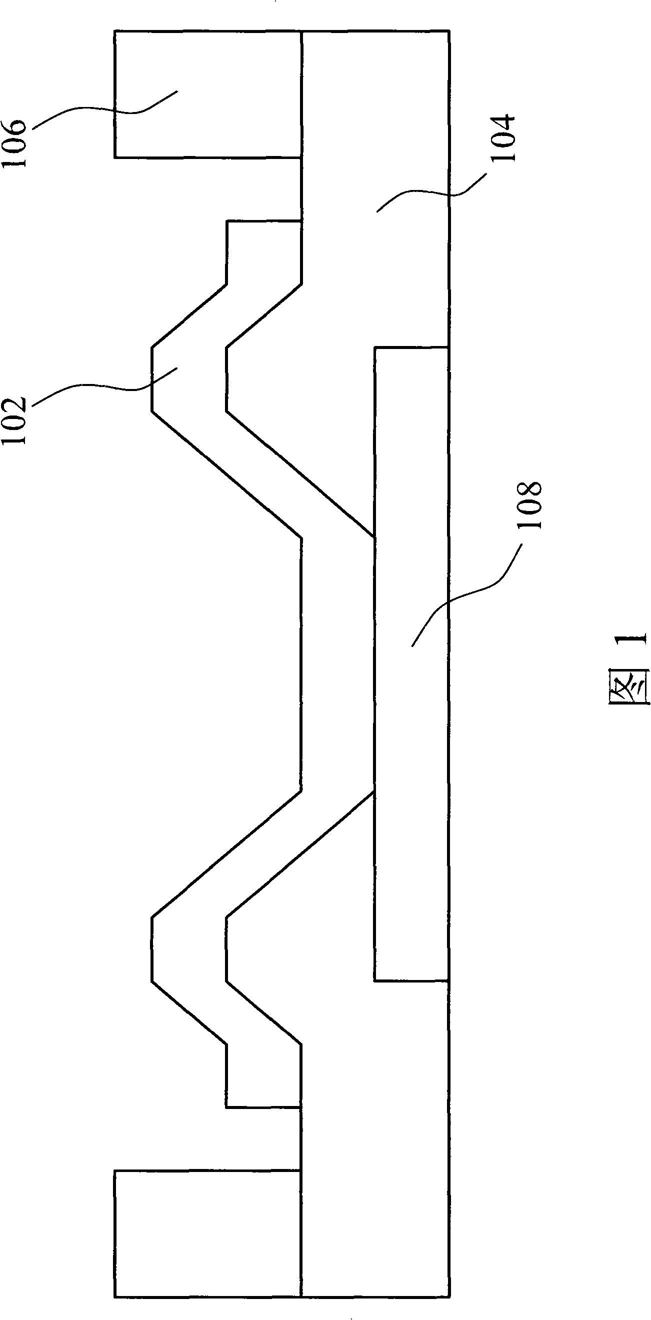
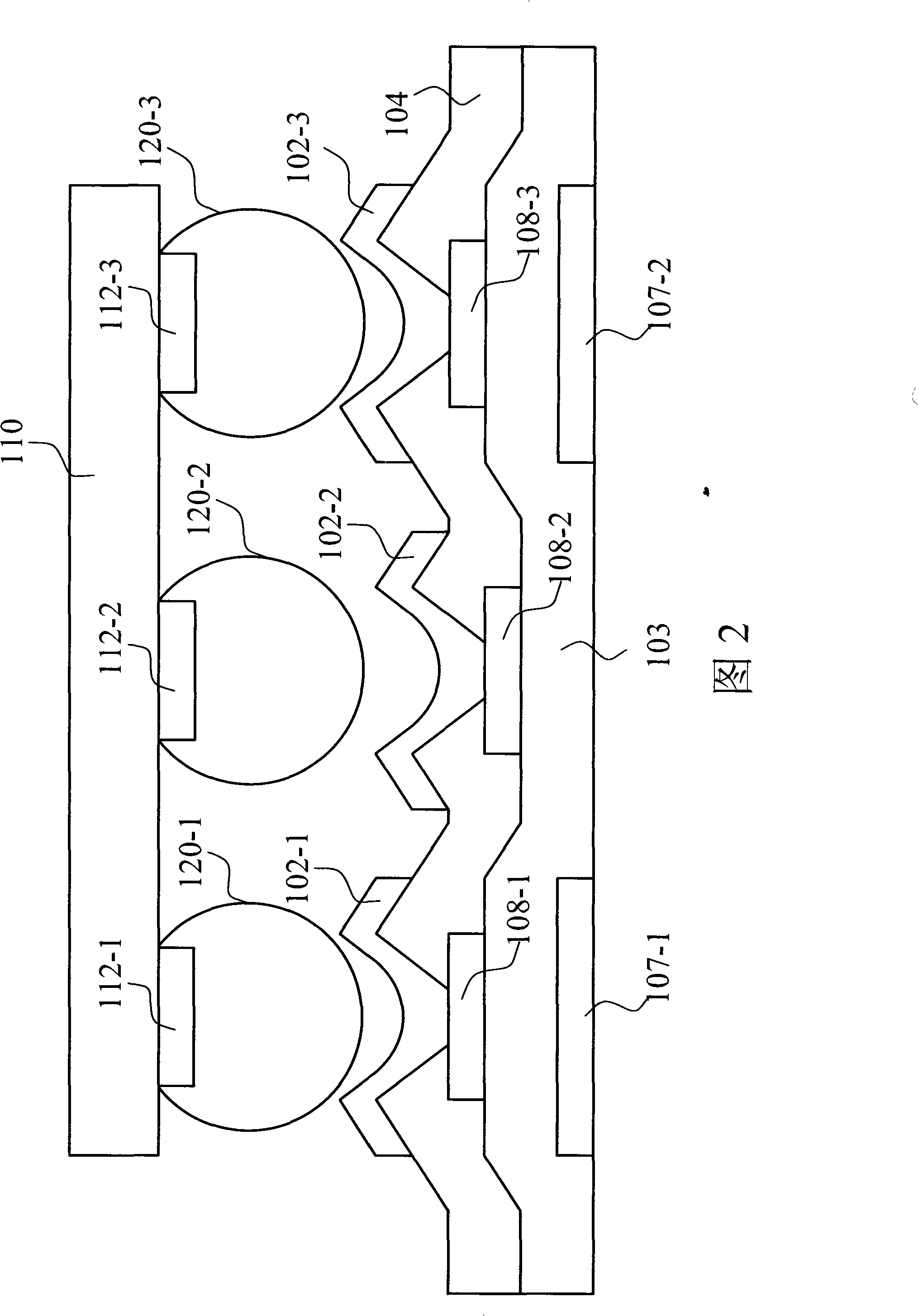
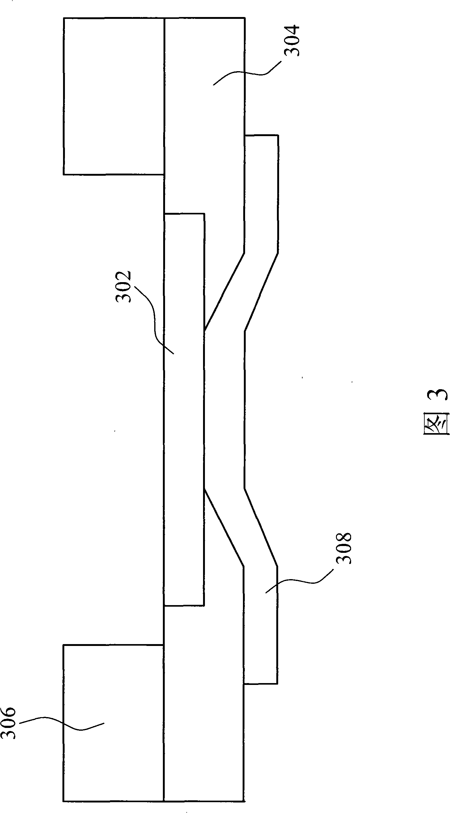
[0023] Please refer to FIG. 3 , which is a simple schematic diagram of the surface of the multilayer substrate of the present invention. The multilayer substrate of the present invention includes at least one pad layer 302 and one surface dielectric layer 304 . Moreover, the multi-layer substrate may further include a solder resist layer 306 . Below the pad layer 302 is a metal circuit layer 308 of the multi-layer substrate. The pad layer 302 of the present invention is embedded in the surface dielectric layer 304 , and the sides of the pad layer 302 are in close contact with the surface dielectric layer 304 , which can enhance the adhesion strength between the two. Furthermore, the surface of the pad layer 302 and the surface of the surface dielectric layer 304 have a coplanarity, so that the surface of the multilayer substrate of the present invention has high flatness, that is, the surface of the pad layer 302 and the surface of the surface dielectric layer 304 There is n...


PUM

PropertyMeasurementUnit
thicknessaaaaaaaaaa
thicknessaaaaaaaaaa

Abstract

The invention discloses a flat multilayer base board and manufacturing method thereof. The multilayer base board of the invention comprises a surface dielectric layer and at least a welding bed layer. The surface dielectric layer is located on a surface of the multilayer base board; the welding bed layer is embedded into the surface dielectric layer, and the surface dielectric layer and the welding bed layer forms the multilayer base board of the invention. The manufacturing method of the invention comprises: forming at least one welding bed layer on a flat carrier board surface; and forming a surface dielectric layer to cover the welding bed layer wile making the welding bed layer embedded in the surface dielectric layer and separating the multilayer base board from the carrier board. Thus, the surface dielectric layer and the welding bed layer forms a multilayer base board with a flat surface.

Description

technical field [0001] The invention relates to a multilayer substrate and its manufacturing method, especially to a flat multilayer substrate and its manufacturing method. Background technique [0002] The miniaturization of any type of electronic products today is an inevitable trend. As the size of the semiconductor wafer process continues to shrink, the related technologies of the back-end packaging must also advance in the direction of miniaturization. Therefore, when the integration level of today's integrated circuits has been continuously increased, it is an inevitable trend to use a multi-layer substrate with a high integration level to package wafers or components and integrate them into a high-density system. [0003] Please refer to FIG. 1 , which is a simple schematic diagram of a multilayer substrate in the prior art. The so-called surface of the multilayer substrate refers to the surface that will be packaged with a chip or component later. The multilayer sub...

Claims


Application Information

Patent Timeline
Patent Type & Authority Patents(China)
IPC IPC(8): H05K1/18H05K3/46H05K1/02
Inventor 杨之光
Owner PRINCO CORP
Why Eureka
Try Eureka