

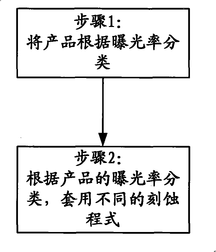
Method for improving etching depth accuracy
A technology of etching depth and accuracy, applied in electrical components, semiconductor/solid-state device manufacturing, circuits, etc., can solve problems such as inaccurate exposure rates, improve production efficiency, avoid scrap, and save manpower and material resources.
- Summary
- Abstract
- Description
- Claims
- Application Information
AI Technical Summary
Problems solved by technology
Method used
Image

Examples
Embodiment Construction
[0014] The present invention will be described in detail below in conjunction with the accompanying drawings and specific embodiments.
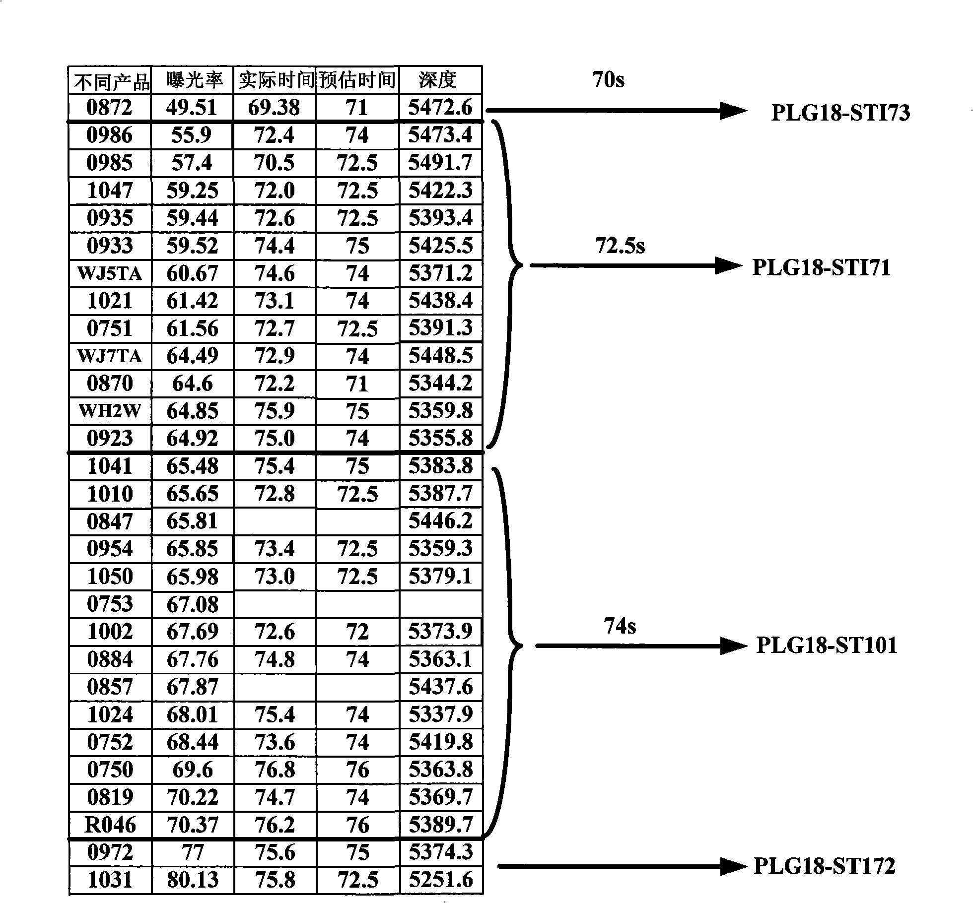
[0015] figure 1 It is a schematic diagram of the program determination of the present invention. The first row of the table represents different products; the second row of the table represents the exposure rate; the third row of the table represents the actual time, that is, the actual etching time required based on experience; the fourth row of the table represents The estimated time is the previously estimated etching time before etching; the fifth column indicates the depth, that is, the etching depth, and the actual time can be obtained according to the mentioned depth. Such as figure 1 As shown, there is a large discrepancy between past estimated times and actual times. In the present invention, different programs are applied to samples from the actual etched products, and the time of the programs is the average value of the actual ti...
PUM
 Abstract
Description
Claims
Application Information