Method for measuring thickness of substrate and equipment for processing substrate

A processing device and thickness measurement technology, applied in measurement devices, grinding devices, optical devices, etc., can solve the problems of unstable interference waves, unstable thickness measurement values, etc., and achieve the effect of stable interference waves

Active Publication Date: 2009-02-25
DISCO CORP
View PDF1 Cites 25 Cited by
  • Summary
  • Abstract
  • Description
  • Claims
  • Application Information

AI Technical Summary

Problems solved by technology

Therefore, the refractive index of the laser light fluctuates or the laser light is difficult to pass through, and the

Method used


Image

  • Method for measuring thickness of substrate and equipment for processing substrate
  • Method for measuring thickness of substrate and equipment for processing substrate
  • Method for measuring thickness of substrate and equipment for processing substrate

Examples


Embodiment Construction

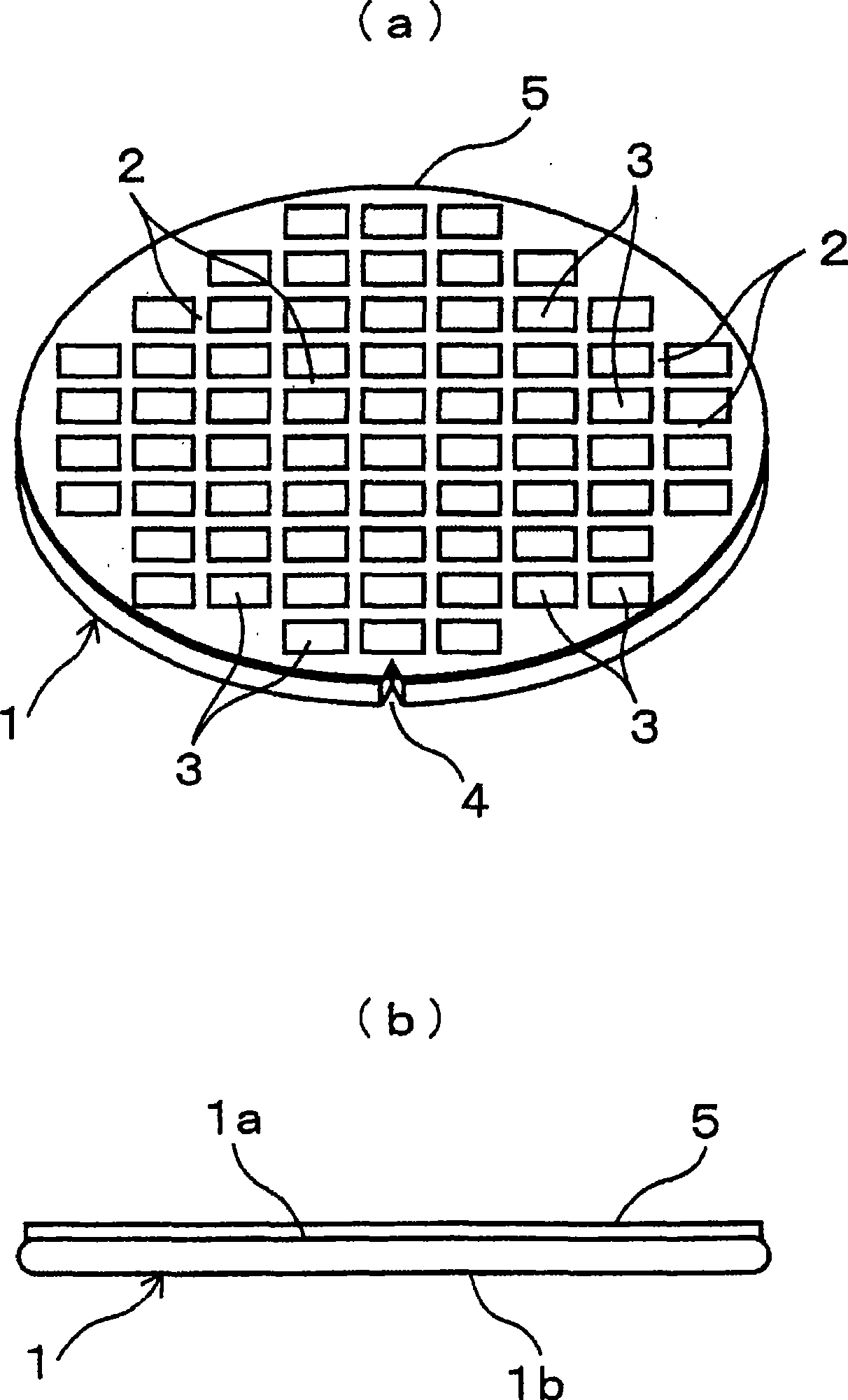
[0034] One embodiment in which the present invention is applied to backside grinding of a semiconductor wafer (substrate) will be described below with reference to the drawings. figure 1 The reference numeral 1 in the figure represents a disk-shaped semiconductor wafer (hereinafter simply referred to as a wafer) thinned by back grinding. This wafer 1 is a silicon wafer or the like, and its thickness before processing is, for example, about 700 μm and is uniform. On the surface (one surface) 1a of the wafer 1, a plurality of rectangular semiconductor chips 3 are divided by grid-like dividing lines 2. As shown in FIG. Electronic circuits (not shown), such as IC (Integrated circuit: integrated circuit) or LSI (large scale integration: large scale integration), are formed on the surfaces of these semiconductor chips 3 . In addition, V-shaped notches (grooves) 4 representing crystal orientations of semiconductors are formed at predetermined positions on the peripheral surface of t...


PUM


Abstract

The invention provides a method for measurement of thickness of a substrate and a processing device for the substrate, when thickness of the substrate is measured by interference of a laser, a stable measurement value is attainable and is not influenced by processing water. A cylindrical shield (74) is connectively arranged on an opening of a laser head portion (70), a wafer (1) is irradiated by the laser (L) from a laser irradiation end (71) on condition that an interior space (75) of the shield (74) is filled with the water 9W) supplied from a water supply pipe (76). The laser (L) irradiates the end (71) to irradiate the wafer (1). The laser (L) irradiates the wafer (1) by permeating through a glass plate (73) of the laser head portion (70) and the water (W) in the interior space (75), thickness of the wafer (1) is detected by means of an interference wave that is generated by reflective lights of a lower surface (surface (1a)) and a processing surface (back (1b)) of the wafer (1). Entry of the grinding water (the processing water) to a laser irradiation region is cut off to maintain the laser irradiation in a fixed state.

Description

technical field [0001] The present invention relates to a processing device for performing processing such as grinding and polishing on a substrate such as a semiconductor wafer, and a method for measuring the thickness of a substrate suitable for such processing. Background technique [0002] In the manufacturing process of a semiconductor device, in order to obtain a target thickness of the device, at the stage of a semiconductor wafer that is an aggregate of a plurality of devices, backside grinding is performed to make it thinner. In response to the remarkable thinning of today's devices, wafers are processed to be thinner, so higher accuracy is required for thickness management. Grinding or grinding of the wafer is performed while measuring the thickness. As a thickness measuring means of this type, a contact type is known in which a measurement probe is brought into contact with a surface to be processed to detect thickness displacement (see Patent Document 1). [000...

Claims


Application Information

Patent Timeline
IPC IPC(8): B24B49/04H01L21/66G01B11/06B24B7/22B24B37/013B24B49/12
Inventor 佐佐木彰法
Owner DISCO CORP
Why Eureka
Try Eureka