Flexible retina salient point micro-electrode chip and production method thereof

A fabrication method and microelectrode technology, applied in the field of microelectromechanical systems, can solve problems such as affecting nerve stimulation or signal recording effect, and inability to achieve electrode site contact, so as to reduce insertion damage, reduce stimulation pulse current, and reduce thermal damage. Effect

Inactive Publication Date: 2009-03-11
SHANGHAI JIAO TONG UNIV
View PDF0 Cites 41 Cited by
  • Summary
  • Abstract
  • Description
  • Claims
  • Application Information

AI Technical Summary

Problems solved by technology

At present, the production of flexible microelectrodes based on polymer materials in the world generally adopts planar technology, which cannot achieve good co

Method used


Image

  • Flexible retina salient point micro-electrode chip and production method thereof
  • Flexible retina salient point micro-electrode chip and production method thereof
  • Flexible retina salient point micro-electrode chip and production method thereof

Examples


Embodiment Construction

[0041] The embodiments of the present invention are described in detail below in conjunction with the accompanying drawings: this embodiment is implemented on the premise of the technical solution of the present invention, and detailed implementation methods and specific operating procedures are provided, but the protection scope of the present invention is not limited to the following the described embodiment.

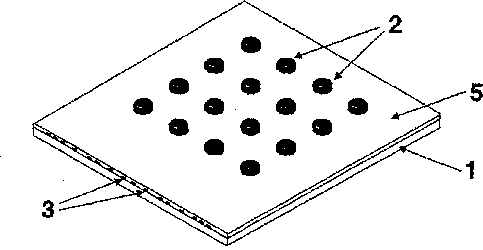
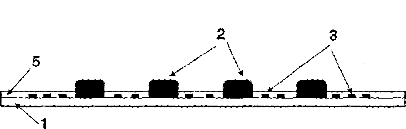
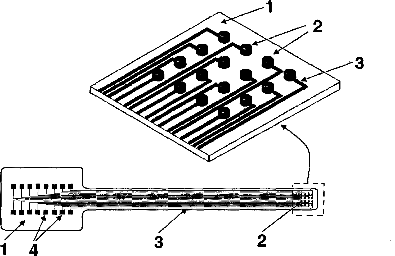
[0042] like figure 1 , figure 2 , image 3 As shown, the present embodiment relates to a flexible retinal bump microelectrode chip, including: a flexible substrate 1, a microelectrode array, an electrode lead 3, a lead solder spot array 4 and an insulating layer 5, wherein the microelectrode array, the electrode lead 3 They are all arranged on a flexible substrate 1, and the microelectrode array is formed by a number of microelectrode sensitive elements 2 arranged in a matrix, and each microelectrode sensitive element 2 is connected to the corresponding solder spot...


PUM

PropertyMeasurementUnit
Heightaaaaaaaaaa
Line widthaaaaaaaaaa
Lengthaaaaaaaaaa

Abstract

The invention discloses a flexible retina emboss micro-electrode chip in the technical field of a micro-electronic-mechanical-system and a manufacture method thereof. In the method, parylene C is used as a flexible substrate and an insulating material for preparing a micro-electrode array which is formed by the arrangement of a plurality of micro-electrode sensing elements; simultaneously, an electrode lead and a lead welding point are manufactured to form the flexible retina emboss micro-electrode chip which is planted into the retina part of a human eye, can realize the safe and effective contact with the neuron of the retina, effectively reduce the stimulation to a pulse current, reduce the inserting damage to a biological tissue caused by the planting of the micro-electrode and can improve the effect of electric simulating and neural signal recording, thereby better recovering the visual function. In the invention, the parylene C is used as the substrate of a flexible electrode; the excellent electric insulating performance and mechanical performance thereof can improve the biocompatibility of the micro-electrode chip to a larger extent and have good stability for a long period. In the invention, an MEMS technique is adopted, thus realizing the integration of a functional unit and the flexible substrate of the micro-electrode.

Description

technical field [0001] The invention relates to a device and a method in the technical field of micro-electromechanical systems, in particular to a flexible retinal bump micro-electrode chip and a manufacturing method thereof. Background technique [0002] The retina is the source of visual function, where light stimuli are converted into visual nerve impulses. For blindness caused by retinal diseases, such as age-related macular degeneration (AMD) and retinitis pigmentosa (RP), implantation of retinal microelectrode chips is a potential means of restoring vision. The basic principle is: the external light signal is sensed by the implant prosthesis, after some specific signal processing, it is converted into a bioelectrical signal, stimulates and activates the optic nerve cells and their connection network, and then transmits the electrical signal to the visual center of the brain through the optic nerve. , resulting in vision. [0003] The flexible retinal microelectrode ...

Claims


Application Information

Patent Timeline
IPC IPC(8): A61F9/08
Inventor 邢玉梅惠春徐爱兰
Owner SHANGHAI JIAO TONG UNIV
Why Eureka
Try Eureka