Method for preparing substrate for growing gallium nitride and method for preparing gallium nitride substrate

A technology of gallium nitride and gallium nitride layer, applied in the field of substrate of semiconductor layer, can solve the problems of time loss and economic loss increase, reduce processing output, process complexity, etc., to reduce processing time, increase processing output, The effect of simplifying the process

Active Publication Date: 2009-03-18
LG SILTRON
View PDF0 Cites 5 Cited by
  • Summary
  • Abstract
  • Description
  • Claims
  • Application Information

AI Technical Summary

Problems solved by technology

Consequently, this can lead to increased processing costs, process complexity, time loss and economic loss, and thus to reduced processing yields

Method used


Image

  • Method for preparing substrate for growing gallium nitride and method for preparing gallium nitride substrate
  • Method for preparing substrate for growing gallium nitride and method for preparing gallium nitride substrate
  • Method for preparing substrate for growing gallium nitride and method for preparing gallium nitride substrate

Examples


Embodiment Construction

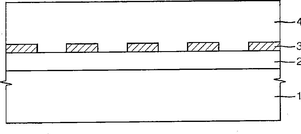
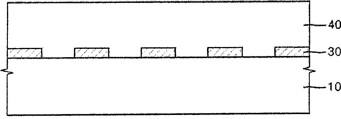
[0025] Hereinafter, specific embodiments will be described in detail with reference to the accompanying drawings. However, this invention may be embodied in different forms and should not be construed as limited to the embodiments set forth herein. Rather, these embodiments are provided so that this disclosure will be thorough and complete, and will fully convey the scope of the invention to those skilled in the art. In the drawings, the shapes of elements are exaggerated for clarity of illustration, and like reference numerals refer to like elements throughout. Those skilled in the art will appreciate that when an element such as a layer is referred to herein as being "on / under" another element, that element can be directly on / under the other element, and one or more intervening elements may also be present. .

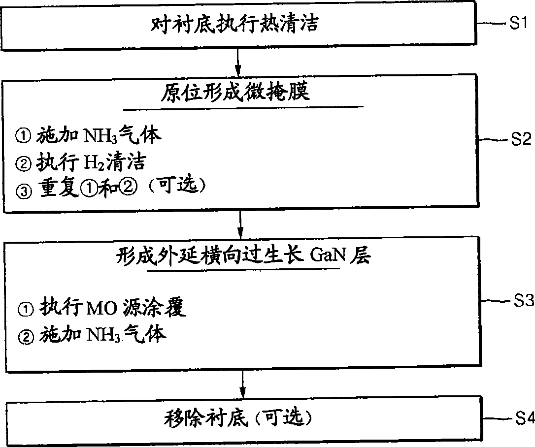
[0026] figure 2 is a flowchart illustrating a method for preparing a substrate for growing gallium nitride and a gallium nitride substrate according to an exempla...


PUM


Abstract

Provided is a method for preparing a substrate for growing gallium nitride and a gallium nitride substrate. The method includes performing thermal cleaning on a surface of a silicon substrate, forming a silicon nitride micro-mask on the surface of the silicon substrate in an in situ manner, and growing a gallium nitride layer through epitaxial lateral overgrowth using an opening in the micro-mask. According to the method, by improving the typical ELO, it is possible to simplify the method for preparing the substrate for growing gallium nitride and the gallium nitride substrate and reduce process cost.

Description

technical field [0001] The present invention relates to a single crystal layer formed of gallium nitride (GaN) or nitrides of gallium and other metals and a method for forming the single crystal layer. The invention also relates to a method of preparing substrates used in the manufacture of electronic or photo-electronic devices comprising single-crystal layers. The present invention relates to the technical field of forming layers of nitride-based semiconductor materials on substrates, and more specifically, the technical field of preparing substrates for forming high-quality nitride-based semiconductor layers. Background technique [0002] Semiconductors based on nitrides of group III elements or group V elements already occupy an important position in the fields of electronics and optoelectronics, and will become more and more important. In fact, nitride-based semiconductors can be used in a wide range of fields, from laser diodes (LDs) to transistors that operate at hig...

Claims


Application Information

Patent Timeline
Patent Type & Authority Applications(China)
IPC IPC(8): H01L21/20H01L21/205H01L33/32
CPCC30B25/18C30B29/406C30B25/02H01L21/20
Inventor 金容进金知勋李东键金杜洙李浩准
Owner LG SILTRON
Why Eureka
Try Eureka