

Wafer stage package cutting method protecting connection pad
A technology of wafer-level packaging and cutting methods, which is applied in the direction of electrical components, semiconductor/solid-state device manufacturing, circuits, etc., and can solve problems such as manual work, cumbersome packaging process, and unsuitability for mass production.
- Summary
- Abstract
- Description
- Claims
- Application Information
AI Technical Summary
Problems solved by technology
Method used
Image

Examples
Embodiment Construction
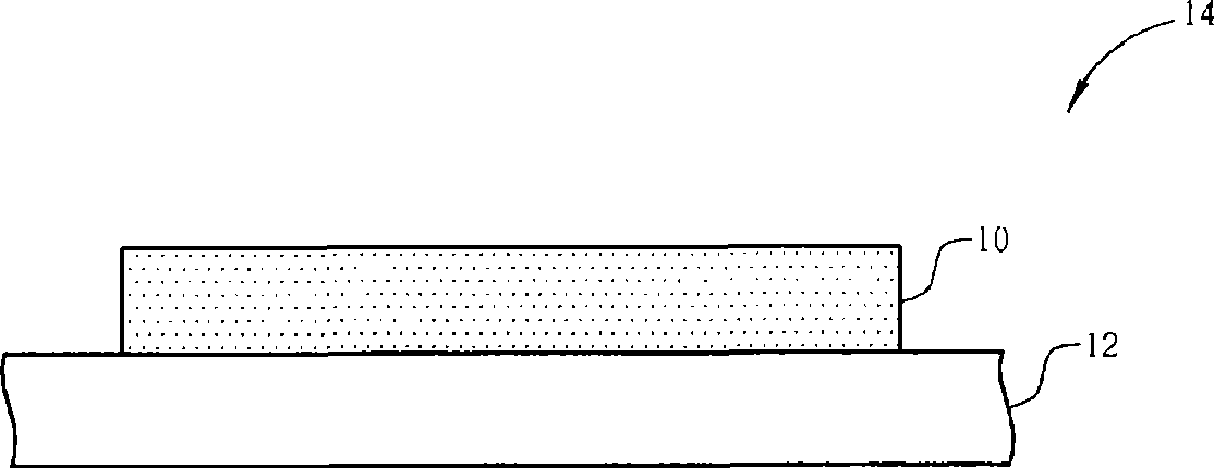
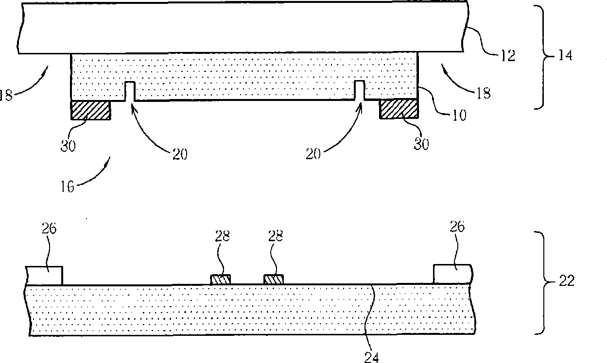
[0024] Please refer to Figure 1 to Figure 6 , Figure 1 to Figure 6 It is a schematic diagram of a wafer dicing manufacturing method according to a preferred embodiment of the present invention. Such as figure 1 As shown, a first wafer 10 and a second wafer 12 are provided through anodic bonding, eutectic bonding, fusion bonding or plasma activation bonding, etc. A known wafer bonding process bonds the first wafer 10 and the second wafer 12 to form a cap wafer 14 . The first wafer 10 can comprise a standard wafer, a silicon wafer, or a wafer with a defined pattern, and the second wafer 12 can be a glass wafer or a packaged wafer, a silicon wafer, or a wafer of other materials. The choice of the chip 14 is not limited to the bonding of two chips as described in this preferred embodiment, and a single standard chip or a silicon chip can also be used as the upper cover chip 14 .
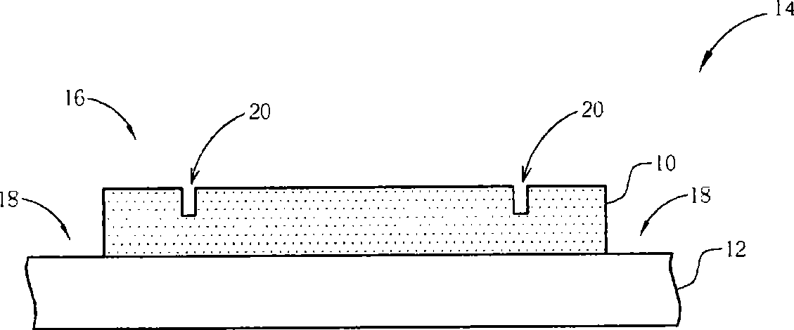
[0025] Such as figure 2 As shown, a surface pattern definition process is performed to simulta...
PUM
| Property | Measurement | Unit |
|---|---|---|
| Line width | aaaaa | aaaaa |
Abstract
Description
Claims
Application Information