Wide forbidden region semi-conductor nano tube/linear array film, preparation and photoelectric pole thereof

A wide-bandgap semiconductor and nanotube technology is applied in the field of solar photoelectric conversion to achieve the effect of improving conversion efficiency

Inactive Publication Date: 2009-03-25
PEKING UNIV
View PDF0 Cites 38 Cited by
  • Summary
  • Abstract
  • Description
  • Claims
  • Application Information

AI Technical Summary

Problems solved by technology

[0006] However, how to fill semiconductor quantum dots into nanotubes to furthe

Method used


Image

  • Wide forbidden region semi-conductor nano tube/linear array film, preparation and photoelectric pole thereof
  • Wide forbidden region semi-conductor nano tube/linear array film, preparation and photoelectric pole thereof
  • Wide forbidden region semi-conductor nano tube/linear array film, preparation and photoelectric pole thereof

Examples


Embodiment Construction

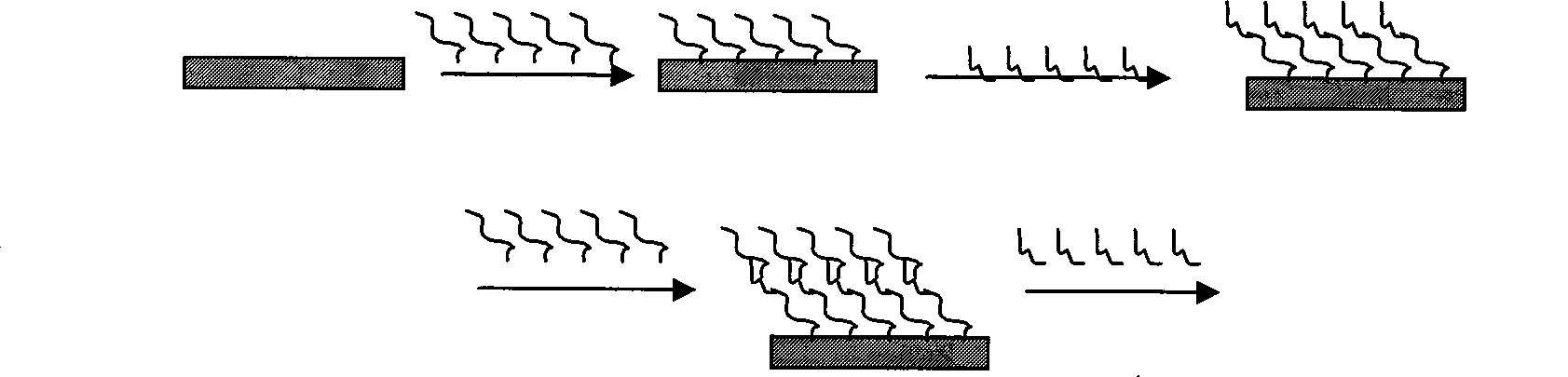
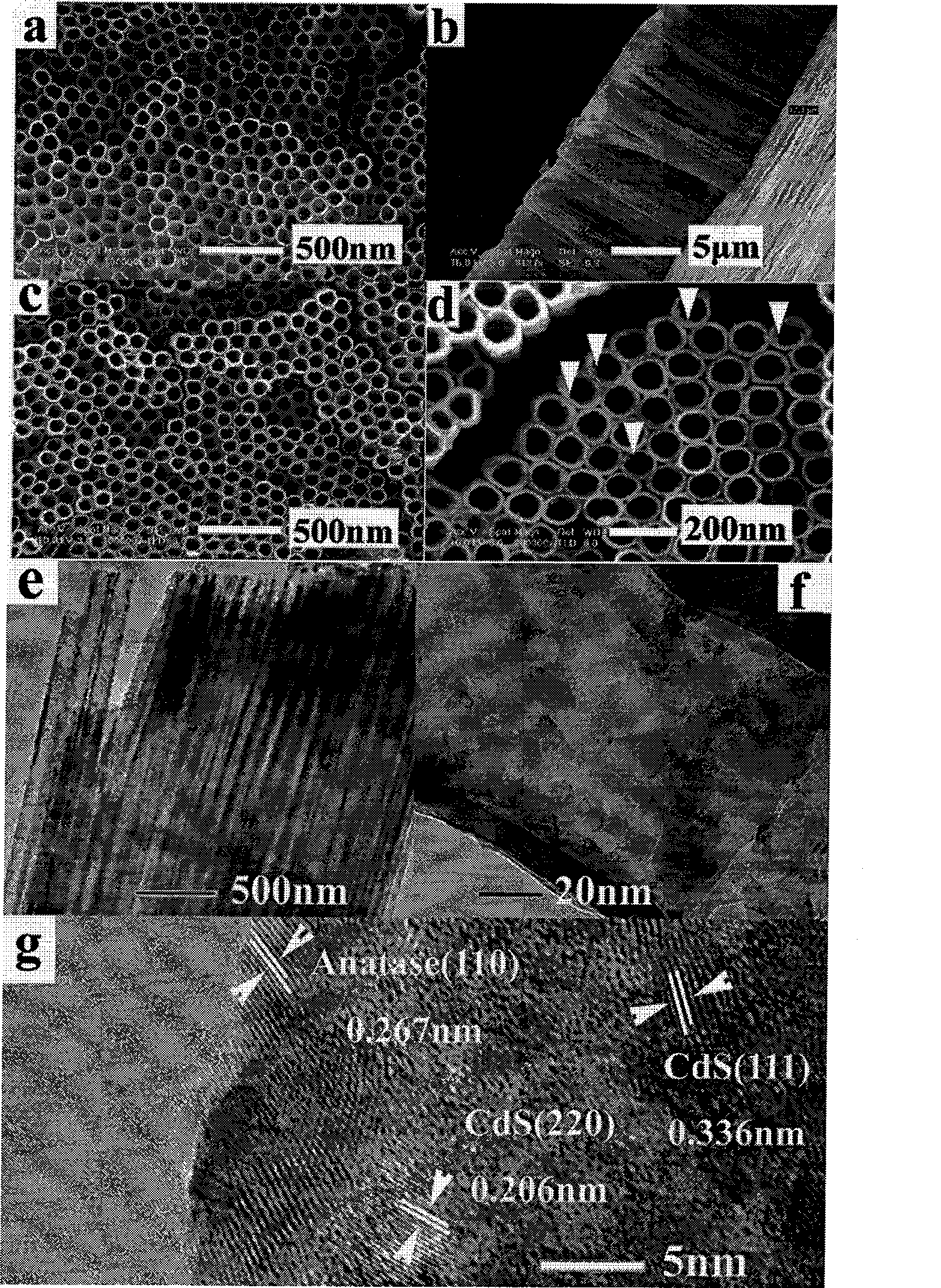
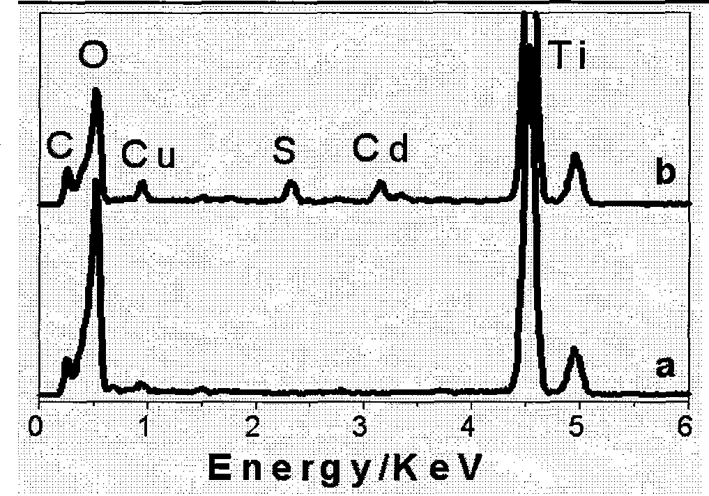
[0031] The invention provides a preparation method and structure of a high-conversion-efficiency quantum dot-sensitized wide-bandgap semiconductor nanotube / line array film solar photoelectrode. The present invention prepares wide-bandgap semiconductor nanotube / line array film by anodic oxidation method (such as in fluorine-containing electrolyte); uses chemical deposition method to prepare wide-gap semiconductor nanotube / line array sensitized by narrow-bandgap semiconductor quantum dots membrane. The photoelectrode using this wide bandgap semiconductor nanotube / line array film is applied in a photoelectrochemical cell, and the photoelectric conversion efficiency is greatly improved, indicating that the narrow bandgap quantum dot and wide bandgap semiconductor nanotube / line array The composite structure can greatly improve the conversion efficiency of photovoltaic cells.

[0032] Next, TiO was sensitized with CdS quantum dots 2 The nanotube (also applicable to nanowire) array...


PUM


Abstract

The invention relates to a wide band gap semiconductor nanotube/line array film characterized by high conversion efficiency and quantum dot sensitization, and a preparation method thereof as well as a photo-electrode adopting the wide band gap semiconductor nanotube/line array film. The wide band gap semiconductor nanotube/line array film provided by the invention comprises a wide band gap semiconductor nanotube/line array and a conductive substrate, and the wide band gap semiconductor nanotube/line array is filled with narrow band gap semiconductor quantum dot nano-particles. According to the preparation method provided by the invention, the anodic oxidation method is used for preparing the wide band gap semiconductor nanotube/line array film, and the chemical deposition method is used for preparing a narrow band semiconductor nanotube/line array film with sensitized quantum dots. The photo-electrode adopting the wide band gap semiconductor nanotube/line array film can be applied to a photo-chemical bath, and the photo conversion efficiency of the photo-chemical bath can be substantially improved. The invention can be widely applied to the technical field of photo-electricity conversion of solar power.

Description

technical field [0001] The invention belongs to the field of photoelectric conversion of solar energy, and in particular relates to a wide-bandgap semiconductor nanotube (or nanowire) array film sensitized by quantum dots with high conversion efficiency and a preparation method thereof, and a method using the wide-bandgap semiconductor nanotube / Line array film photoelectrodes. Background technique [0002] Entering the 21st century, with the further development of human civilization and the rapid growth of the world population, the energy crisis and environmental pollution caused by it have become serious problems that need to be solved urgently, which makes human beings have a greater demand for the development and utilization of clean new energy. As a renewable energy source, solar energy has advantages that other energy sources cannot match: it is inexhaustible, does not cause ecological environmental pollution, is low in cost, and has huge power. Solar cells are one of...

Claims


Application Information

Patent Timeline
IPC IPC(8): H01L31/0224H01L31/18H01G9/042H01G9/20H01M14/00H01M4/02H01M4/04
CPCY02E60/10Y02P70/50
Inventor 孙文涛彭练矛
Owner PEKING UNIV
Why Eureka
Try Eureka