Semiconductor array laser light beam reshaping structure

A beam shaping and semiconductor technology, which is applied in the laser field, can solve the problems of large divergence angle, short working distance, and underutilization of the beam, and achieve the effect of small divergence angle, large spot diameter and long working distance

Inactive Publication Date: 2009-04-08
SHANGHAI BRANCH FUZHOU GAOYI COMM CO LTD
View PDF0 Cites 15 Cited by
  • Summary
  • Abstract
  • Description
  • Claims
  • Application Information

AI Technical Summary

Problems solved by technology

Semiconductor laser arrays generally have 20 to 60 chips per 1 cm. The collimation system using an ordinary microlens array will result in a small diameter of the collimated spot, a large divergence angle, and a short working distance, and the beam will not be fully utilized.

Method used


Image

  • Semiconductor array laser light beam reshaping structure
  • Semiconductor array laser light beam reshaping structure
  • Semiconductor array laser light beam reshaping structure

Examples


Embodiment approach 1

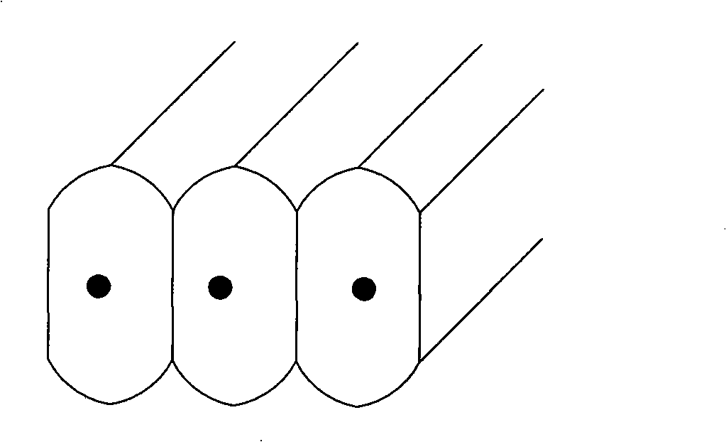
[0032] Such as figure 1 As shown, the optical element structure is a semiconductor laser array 101 , a collimating lens array 102 , a cylindrical mirror 103 and a beam changing prism 104 arranged in sequence.

[0033] The laser light is emitted from the semiconductor laser, and first passes through the collimating lens array to shape the beam in a 10° direction. The focal length of the lens is as large as possible, and it is close to the limit of the size of the collimated beam at an angle of 10°, that is, it is smaller than and close to the center distance between two chips. , to maximize the spot size. After further compressing the long-axis direction of the output beam of the semiconductor laser by a prism, a prism pair or a grating, it can be coupled directly or through a converging lens to a multimode fiber, a high-power fiber or directly used in an end-pumped laser.

Embodiment approach 2

[0035] Such as figure 2 As shown, the optical element structure is a semiconductor laser array 201 , a collimating lens array 202 , a cylindrical mirror 203 , a pair of beam changing prisms 204 and 205 , a coupling lens 206 and an optical fiber 207 .

[0036] Whether the coupling lens 206 is needed depends on the specific conditions of the diameter of the compressed beam.

Embodiment approach 3

[0038] Such as image 3 As shown, the optical element structure is a semiconductor laser array 301 , a cylindrical mirror 302 , a beam changing grating 303 , a coupling lens 304 and an optical fiber 305 arranged in sequence.

[0039] After the laser light emitted by the semiconductor laser is collimated and compressed by the cylindrical mirror 302 and the variable beam grating 303 , it can be coupled into the optical fiber 305 through a coupling lens or directly.


PUM


Abstract

The invention relates to the field of laser, in particular to a light beam shaping structure of a semiconductor array laser which adopts a self-focusing lens with special structure, a non-spherical lens, a spherical lens or array and a cylindrical lens or a combination of cylindrical lenses to reshape all the luminous points into parallel light beams having minimized angle, high power compression is carried out on semiconductor light beam along the direction of prolate axis by adopting a single prism, a combination of prisms or raster array, and the obtained light beam can be directly and effectively coupled to multimode fiber and high power doubly coated fiber, or used in an end pump laser, or the obtained light beam can be effectively coupled to multimode fiber and high power doubly coated fiber, or used in an end pump laser by passing through a plus lens. The invention is a novel light beam shaping structure of the semiconductor laser and has the advantages of larger spot diameter of the output beam, smaller divergence angle and further operating distance.

Description

technical field [0001] The invention relates to the laser field, in particular to a beam shaping structure of a semiconductor array laser. Background technique [0002] Semiconductor lasers are widely used in many fields such as solid-state lasers pumped by semiconductor lasers, fiber lasers, and material processing due to their advantages such as high light conversion efficiency, narrow linewidth, stable and reliable performance, small size, and light weight. However, due to its special working principle, the beam quality of semiconductor lasers is very different in the two directions perpendicular to and parallel to the P-N junction. In practical applications (such as fiber coupling), it is necessary to shape the beam to form a small core diameter. High brightness fiber-coupled semiconductor laser output with small numerical aperture. [0003] Commonly used beam shaping methods include: multiple optical fibers are individually coupled into a fiber bundle, or coupled with ...

Claims


Application Information

Patent Timeline
Patent Type & Authority Applications(China)
IPC IPC(8): H01S5/40G02B27/09G02B27/30
Inventor 吴砺邱英凌吉武
Owner SHANGHAI BRANCH FUZHOU GAOYI COMM CO LTD
Why Eureka
Try Eureka