Production process for golden electrode for LED
A technology of light-emitting diodes and gold electrodes, which is applied in the field of preparation of gold electrodes for light-emitting diodes, to achieve the effects of stable storage, high purity, and no pinhole cracks
- Summary
- Abstract
- Description
- Claims
- Application Information
AI Technical Summary
Problems solved by technology
Method used
Image

Examples
Embodiment 1
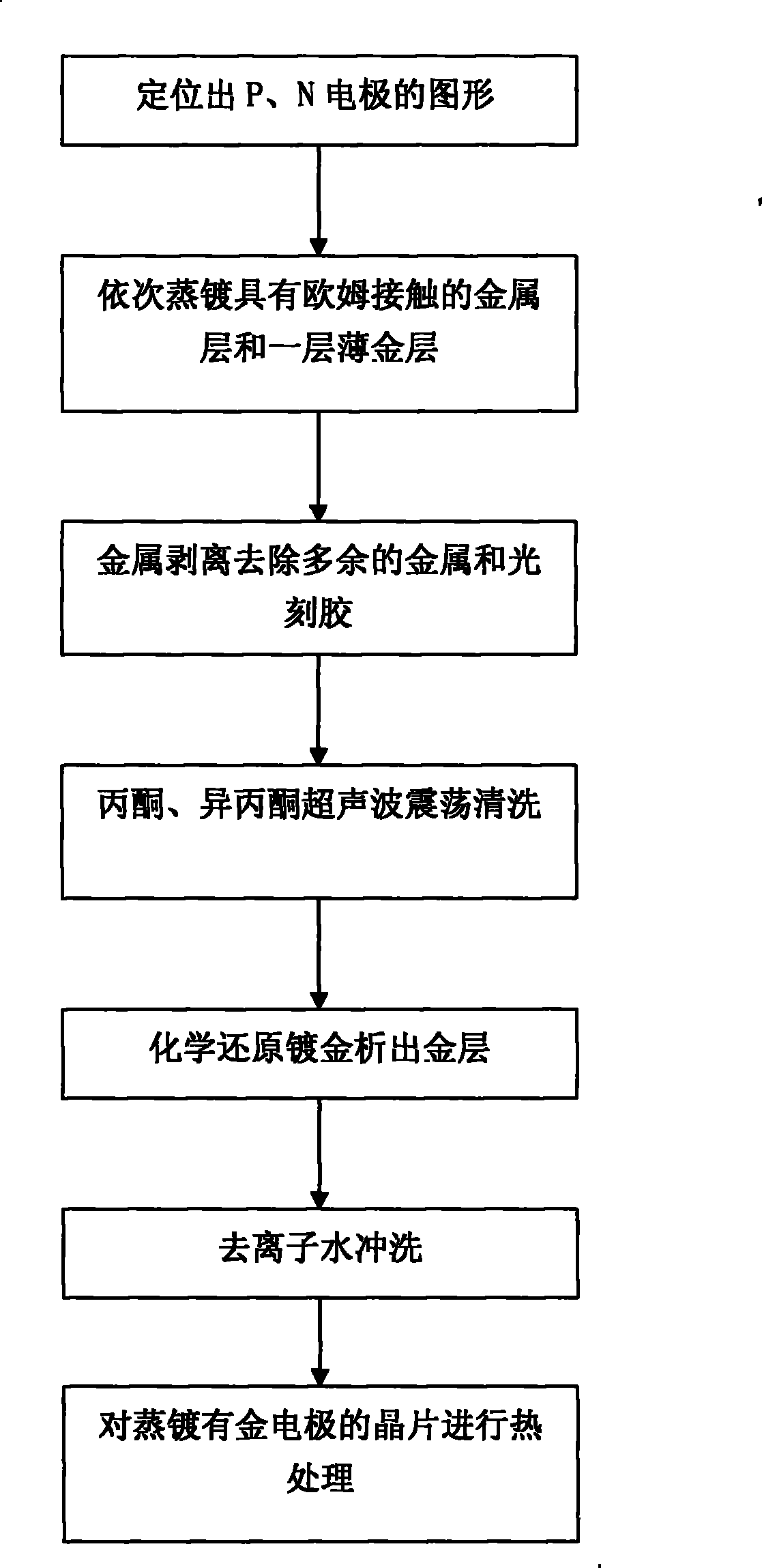
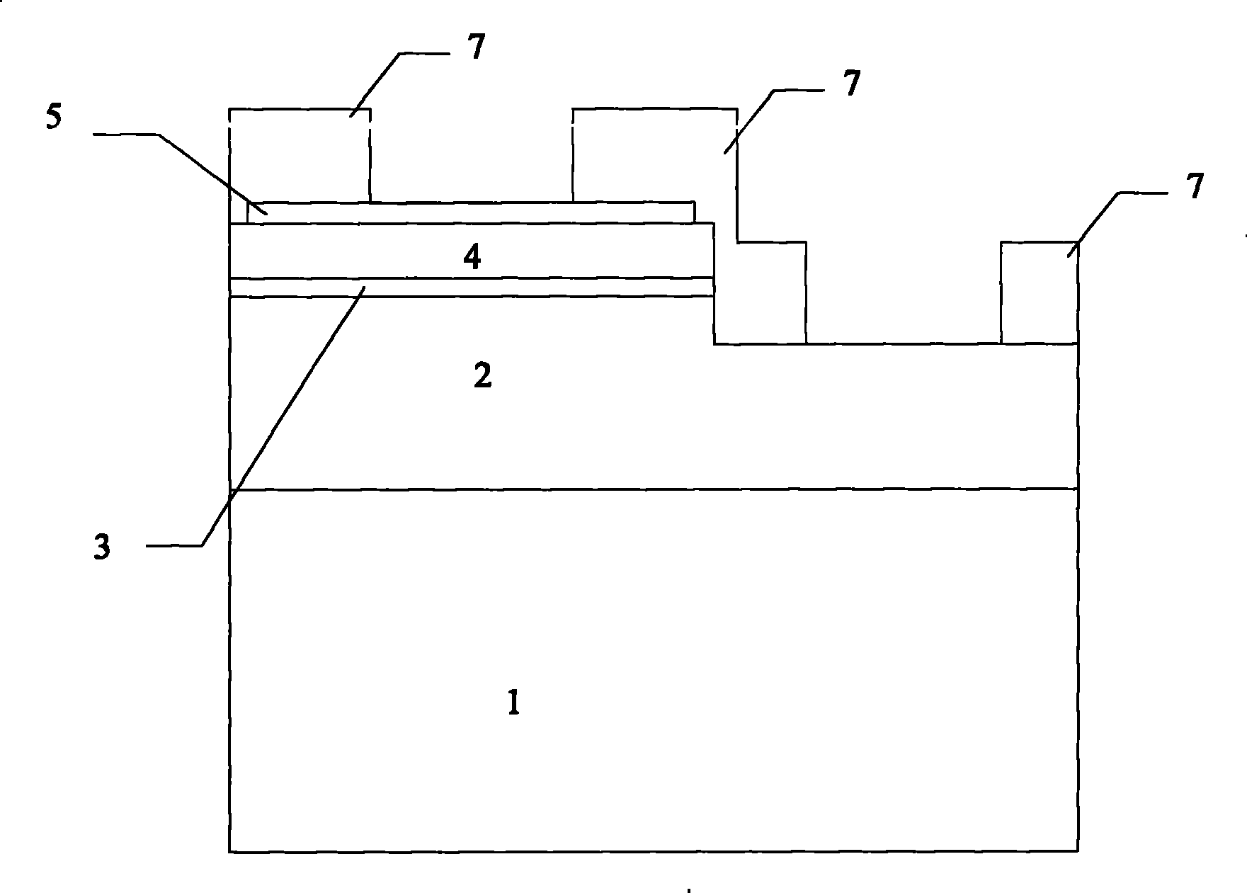
[0043] (2) On the transparent electrode layer 5, the N-type layer 2, the metal layer with ohmic contact and a layer of gold 8 with a thickness of 300 angstroms are evaporated successively, as image 3 Shown; remove excess photoresist and metal by Lift-off, then clean the wafer with acetone and isopropanone ultrasonic vibration to remove residual photoresist and organic matter;
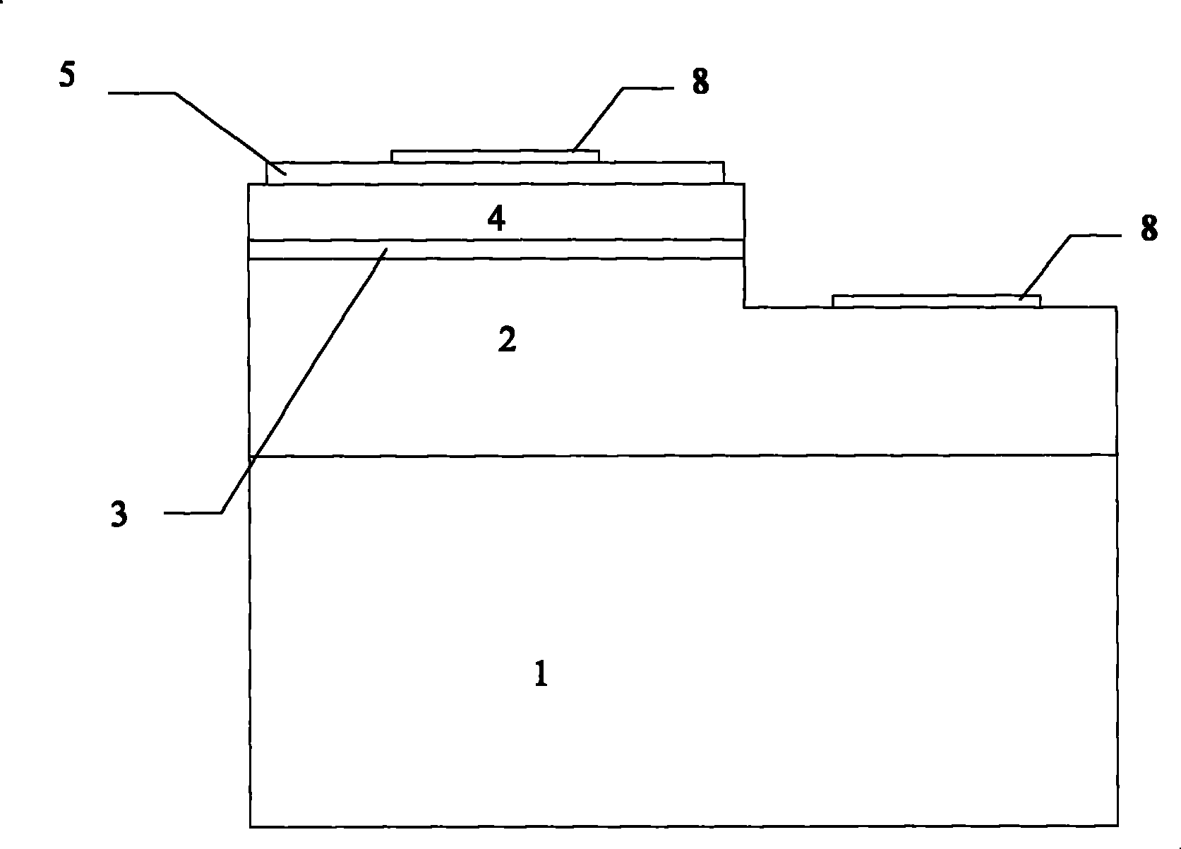
[0044] (3) Under the conditions of 5g / L of gold sodium sulfite (calculated as gold), the chemical gold plating solution component, the pH value is 7.5, and the temperature is 50°C, the deposition thickness on the surface of the evaporated gold layer by reduction reaction is 10000 EGG 9, such as Figure 4 shown;
[0045] (4) Rinse and clean the wafer alternately with hot and cold deionized water; in an alloy furnace fed with 10 sccm nitrogen, the temperature is 225° C., and the wafer for which the gold electrode is prepared is subjected to heat treatment for 15 min.
[0046] The gold electrode prepare...
Embodiment 2
[0050] (2) On the transparent electrode layer 5, the N-type layer 2, the metal layer with ohmic contact and a layer of gold 8 with a thickness of 500 angstroms are evaporated successively, as image 3Shown; remove excess photoresist and metal by Lift-off, then clean the wafer with acetone and isopropanone ultrasonic vibration to remove residual photoresist and organic matter;
[0051] (3) Under the conditions of 5 g / L of sodium gold sulfite (calculated as gold) in the electroless gold plating solution component, the pH value is 7.8, and the temperature is 60° C., the deposition thickness of the evaporated gold layer is 15,000 μm by reduction reaction. Angstrom 9, such as Figure 4 shown;
[0052] (4) Rinse and clean the wafer alternately with hot and cold deionized water; in an alloy furnace fed with 10 sccm nitrogen gas, the temperature is 250° C., and the wafer for which the gold electrode is prepared is subjected to heat treatment for 15 min.
[0053] The gold electrode p...
Embodiment 3
[0057] (2) On the transparent electrode layer 5, the N-type layer 2, the metal layer with ohmic contact and a layer of gold 8 with a thickness of 400 angstroms are evaporated successively, as Figure 6 Shown; remove excess photoresist and metal by Lift-off, then clean the wafer with acetone and isopropanone ultrasonic vibration to remove residual photoresist and organic matter;
[0058] (3) Under the conditions of 5g / L gold sodium sulfite (calculated as gold), the chemical gold plating solution component, the pH value is 7.5, and the temperature is 55°C, the deposition thickness on the evaporated gold layer surface by reduction reaction is 10000 Angstrom 9, such as Figure 7 as shown,
[0059] (4) Rinse and clean the wafer alternately with hot and cold deionized water; in an alloy furnace fed with 10 sccm nitrogen, the temperature is 225° C., and the wafer for which the gold electrode is prepared is subjected to heat treatment for 15 min.
[0060] The gold electrode prepared...
PUM
| Property | Measurement | Unit |
|---|---|---|
| thickness | aaaaa | aaaaa |
| thickness | aaaaa | aaaaa |
| hardness | aaaaa | aaaaa |
Abstract
Description
Claims
Application Information
 - R&D
- Intellectual Property
- Life Sciences
- Materials
- Tech Scout
- Unparalleled Data Quality
- Higher Quality Content
- 60% Fewer Hallucinations
Browse by: Latest US Patents, China's latest patents, Technical Efficacy Thesaurus, Application Domain, Technology Topic, Popular Technical Reports.
© 2025 PatSnap. All rights reserved.Legal|Privacy policy|Modern Slavery Act Transparency Statement|Sitemap|About US| Contact US: help@patsnap.com