Semiconductor element and device using the same
A technology of semiconductors and components, which is applied in the field of semiconductor components and devices using the semiconductor components, and can solve problems such as inappropriate mass production and reduced memory reliability
- Summary
- Abstract
- Description
- Claims
- Application Information
AI Technical Summary
Problems solved by technology
Method used
Image
Examples
no. 1 approach
[0134] In the following description, two states related to information storage, a so-called write state and an erase state, are defined as follows.
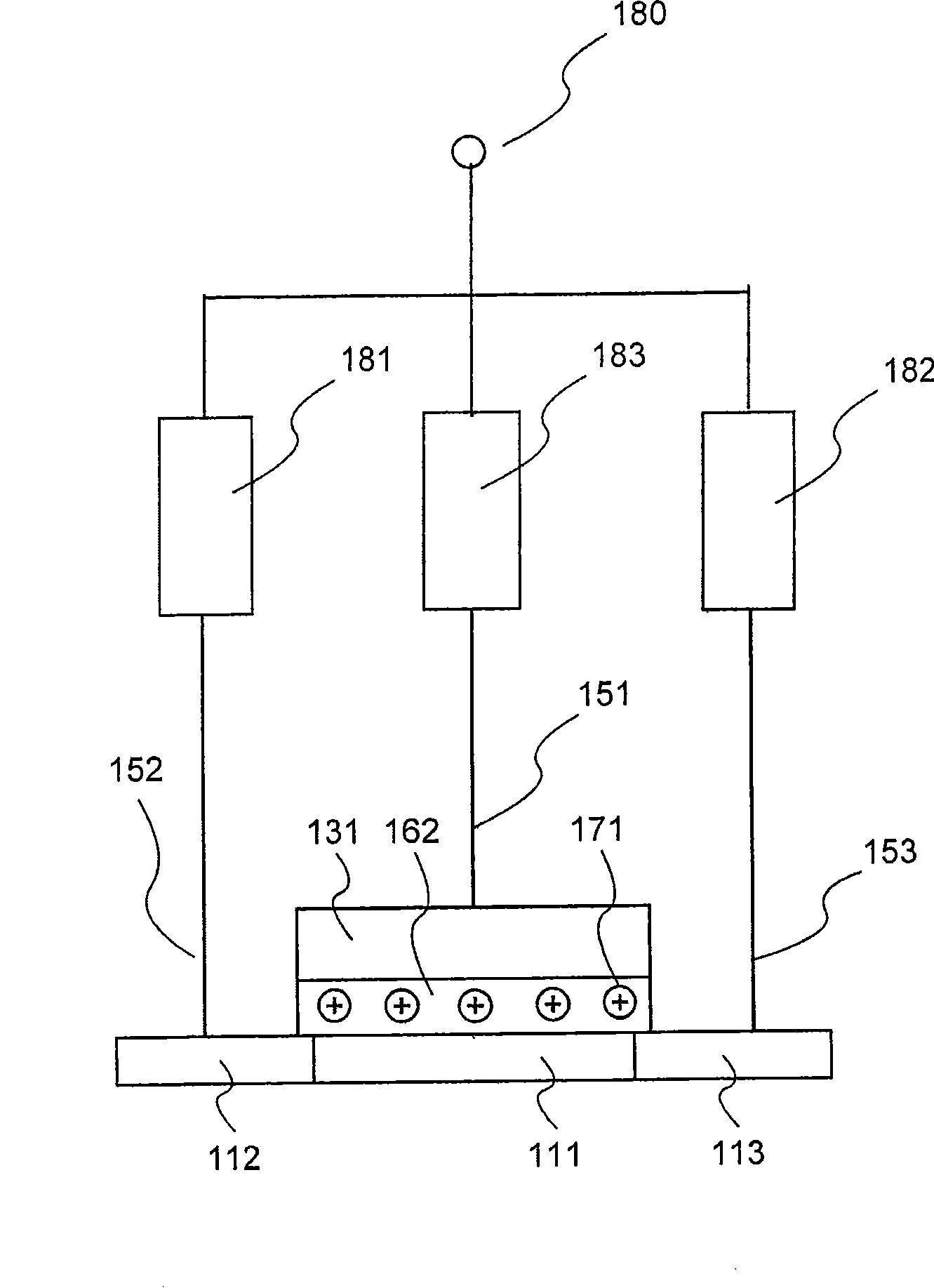
[0135] A state in which most carriers of the conductivity type of the first and second diffusion layer regions are mainly accumulated in the gate insulating film having a function of accumulating charges is defined as a written state. Furthermore, a case where carriers of a type opposite to the conductivity type are mainly accumulated, or a case where the accumulated charge is practically small is defined as an erased state. Both the holes and the electrons are accumulated and the potentials of each other cancel each other out, so that there is actually a small amount of accumulated charge.
[0136] The semiconductor element of the present invention is a P-channel type semiconductor element in which the first and second diffusion layer regions are P-type. In this case, the state in which holes are mainly accumulated in the gate ...
no. 2 approach
[0232] A second embodiment of the present invention will be described using FIG. 11 .
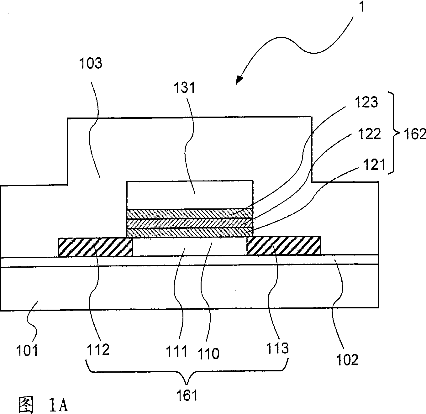
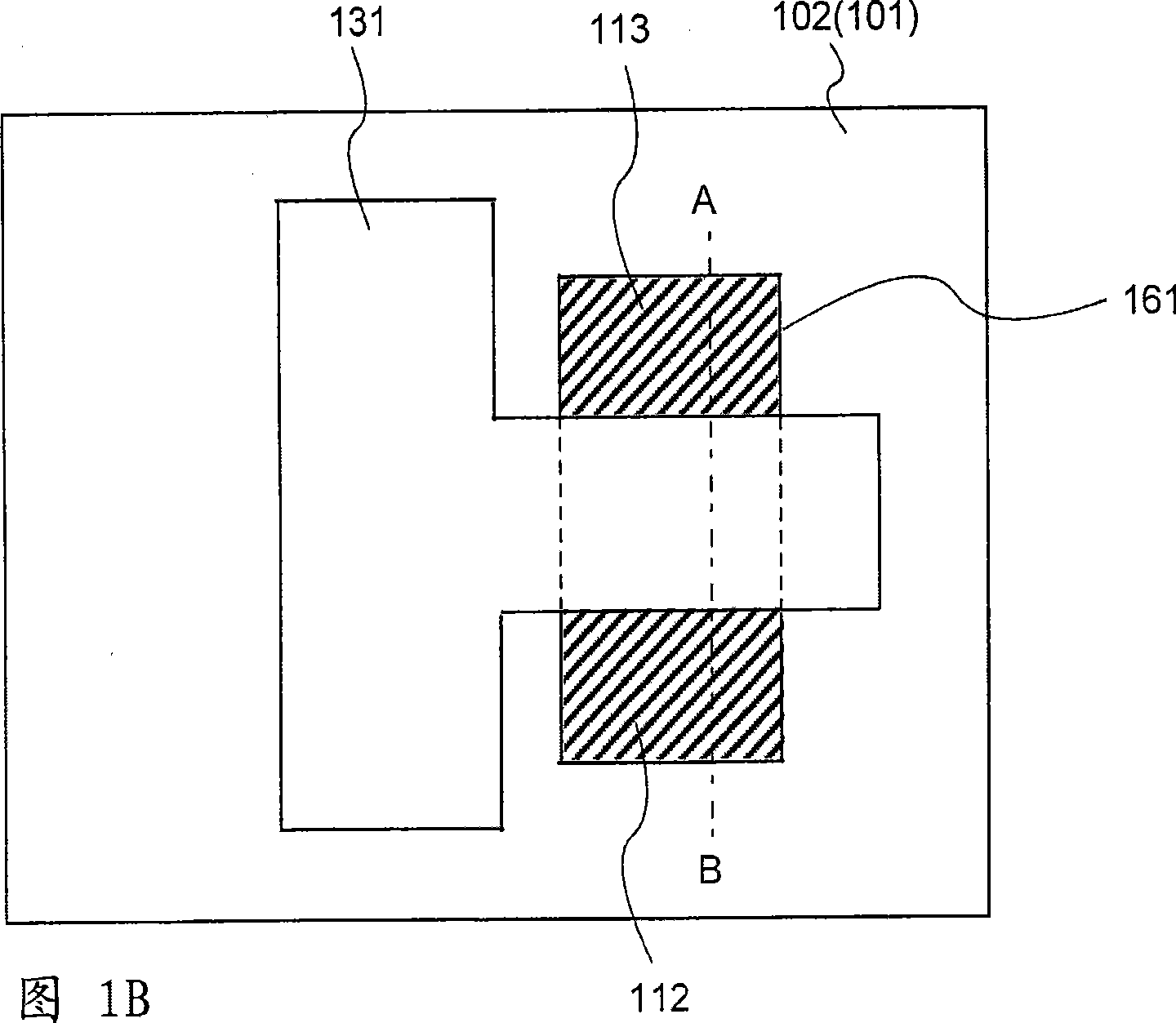
[0233] FIG. 11A is a schematic cross-sectional view along line A-B of FIG. 11B , and FIG. 11C is a schematic plan view. The cross-sectional structure is the same as that of the above-mentioned first embodiment. The body region 111 and the P-type diffusion layer regions 112 and 113 are provided in the semiconductor layer 161, and the surface of the body region 111 between the P-type diffusion layer regions 112 and 113 becomes a channel. The region 110 further has a charge storage film 162 and a gate electrode 131 on its upper portion.
[0234] Here, the second embodiment is characterized in that it includes an electrode terminal (not shown) that is in contact with the body region 111 and controls the potential of the body region. As a particularly preferred manner, as shown in FIG. 11B as an example, a part of the body region 111 is a body contact region 114 with N-type conductivity, and th...
no. 3 approach
[0288] In a third embodiment of the present invention, the memory element described in the above-mentioned embodiments 1 and 2 is used in a liquid crystal display device.
[0289] A liquid crystal display device is composed of a pair of substrates with liquid crystals separated, such as Figure 25A As shown, a scanning line 512 and a signal line 513 are formed on a substrate, and the area surrounded by the scanning line 512 and the signal line 513 is a pixel, and a driving circuit for selectively driving the pixel electrode corresponding to the pixel is provided. 510. Each pixel electrode is opposite to an opposite electrode formed on another substrate, and a liquid crystal exists between them, and one pixel is selectively driven.
[0290] The third embodiment is characterized in that the memory element described in the first embodiment is formed on the panel substrate of the liquid crystal display device. In this case, the memory element of the present invention is used as ...
PUM
| Property | Measurement | Unit |
|---|---|---|
| thermal conductivity | aaaaa | aaaaa |
| thickness | aaaaa | aaaaa |
| thermal conductivity | aaaaa | aaaaa |
Abstract
Description
Claims
Application Information


