A universal non-volatile write-once-read-many memory and its preparation method
A non-volatile, multiple-read technology, applied in the direction of electrical components, etc., can solve the problems of restricting extensive development, complex preparation process, resistive storage performance, etc., and achieve large storage window value, simple preparation steps, and stability high effect
- Summary
- Abstract
- Description
- Claims
- Application Information
AI Technical Summary
Problems solved by technology
Method used
Image
Examples
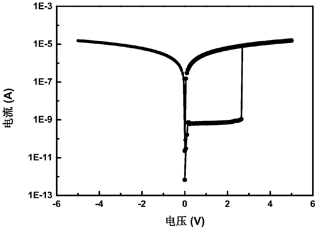
Embodiment 1
[0035] A method for preparing a universal non-volatile write-once-read-many memory, comprising the following steps:
[0036] (1) Substrate treatment: Sonicate the silicon wafer substrate with ethanol, isopropanol, and ethanol for 10 minutes, blow dry with nitrogen, and then treat it with an oxygen plasma cleaner at a power of 50W for 3 minutes.
[0037] (2) Preparation of the bottom electrode: Spin-coat the graphene oxide solution on the silicon wafer substrate first to obtain a large-area graphene oxide film, and then reduce it at a high temperature of 1000°C for 2 hours in an argon / hydrogen mixed atmosphere to obtain Reduced graphene oxide film.
[0038] (3) Preparation of the storage medium layer: the insulating polymer PMMA was dissolved in toluene solution, and then spin-coated on the bottom electrode, the rotation speed of the spin coater was 1000rpm, and dried, and the thickness of the storage medium layer was 70nm;
[0039] (4) Preparation of the top electrode: by the...
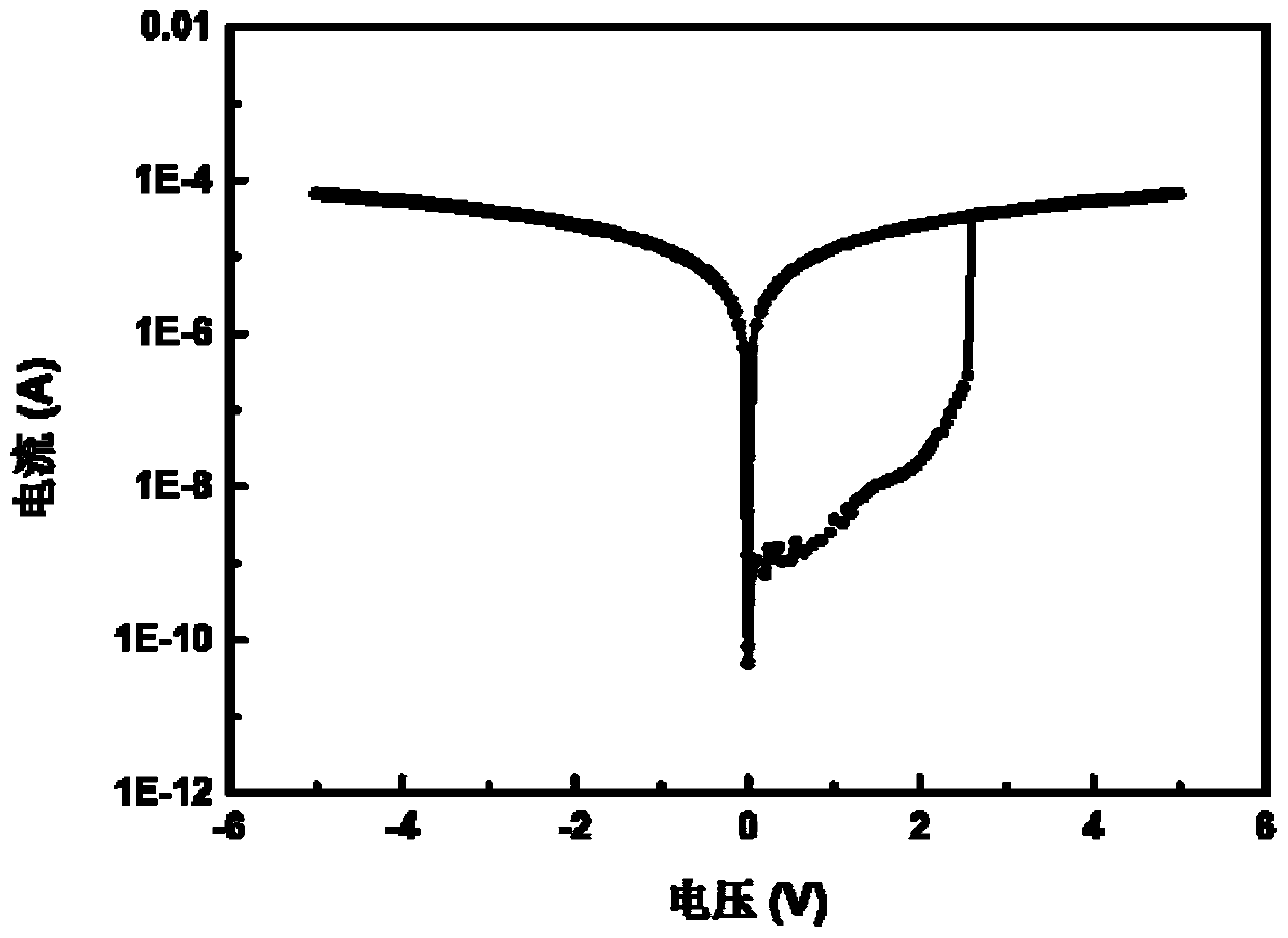
Embodiment 2
[0042] A method for preparing a universal non-volatile write-once-read-many memory, comprising the following steps:
[0043] (1) Substrate treatment: Sonicate the silicon wafer substrate with ethanol, isopropanol, and ethanol for 15 minutes, blow dry with nitrogen, and then treat it with an oxygen plasma cleaner at a power of 30W for 5 minutes.
[0044] (2) Preparation of the bottom electrode: Spin-coat a graphene oxide solution on a silicon wafer substrate first to obtain a large-area graphene oxide film, and then reduce it at a high temperature of 1100°C for 1.5 hours in an argon / hydrogen mixed atmosphere to obtain Reduced graphene oxide film.
[0045] (3) Preparation of the storage medium layer: Dissolve the insulating polymer PS in the dichlorobenzene solution, and then spin-coat it on the bottom electrode. The rotation speed of the spin coater is 800rpm, and dry it. The thickness of the storage medium layer is 75nm;
[0046] (4) Preparation of the top electrode: by therm...
Embodiment 3
[0049] A method for preparing a universal non-volatile write-once-read-many memory, comprising the following steps:
[0050] (1) Substrate treatment: Sonicate the silicon substrate with ethanol, isopropanol, and ethanol for 20 minutes, blow dry with nitrogen, and then treat it with an oxygen plasma cleaner at a power of 10W for 8 minutes.
[0051] (2) Preparation of the bottom electrode: Spin-coat a graphene oxide solution on a silicon wafer substrate first to obtain a large-area graphene oxide film, and then reduce it at a high temperature of 1200°C for 1 hour in an argon / hydrogen mixed atmosphere to obtain Reduced graphene oxide film.
[0052] (3) Preparation of the storage medium layer: Dissolve the insulating polymer PVP in an ethanol solution, and then spin-coat it on the bottom electrode. The rotation speed of the spin coater is 1200rpm, and dry it. The thickness of the storage medium layer is 65nm;
[0053] (4) Preparation of the top electrode: by thermal evaporation, ...
PUM
 Abstract
Description
Claims
Application Information


