Preparation method and application of INP resistive memory material

A resistive variable storage and equipment technology, which is applied in metal material coating process, vacuum evaporation plating, coating, etc., can solve the problems such as the difficulty of process implementation and will not be quickly promoted, and achieve improved defect status, high durability, and improved The effect of shift consistency

Active Publication Date: 2019-08-20
GRIMAT ENG INST CO LTD
View PDF4 Cites 0 Cited by
  • Summary
  • Abstract
  • Description
  • Claims
  • Application Information

AI Technical Summary

Problems solved by technology

However, the reduction of device size will eventually reach the physical limit, and there are many problems in the reliability and other performance of multi-valued storage technology, while 3D technology faces many difficult challenges such as material selection, device structure, and process realization difficulty. It will not be promoted rapidly for the time being. Therefore, in order to achieve higher data storage density and lower unit bit cost, a new type of memory structure that is highly compatible with CMOS technology is urgently needed.

Method used


Image

  • Preparation method and application of INP resistive memory material
  • Preparation method and application of INP resistive memory material
  • Preparation method and application of INP resistive memory material

Examples


preparation example Construction

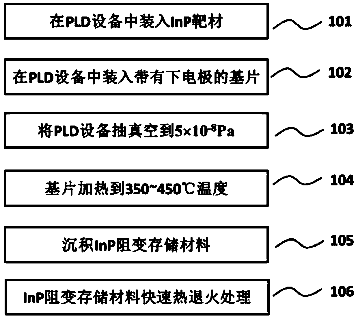
[0024] figure 1 Flowchart for the preparation method of InP resistive memory material:

[0025] Step 101: loading a single crystal InP sheet as a target into a cavity of a pulsed laser device;

[0026] Step 102: loading the substrate with electrodes deposited on the surface into the cavity of the pulsed laser device;

[0027] Step 103: Vacuumize the cavity of the pulsed laser equipment to 5×10 -8 Pa;

[0028] Step 104: heating the substrate to 350-450°C;

[0029] Step 105: Depositing an InP thin film on the substrate by means of pulsed laser deposition;

[0030] Step 106: performing rapid thermal annealing on the substrate deposited with the InP thin film at 600-800° C. for 5-120 seconds to obtain an InP resistive memory material.

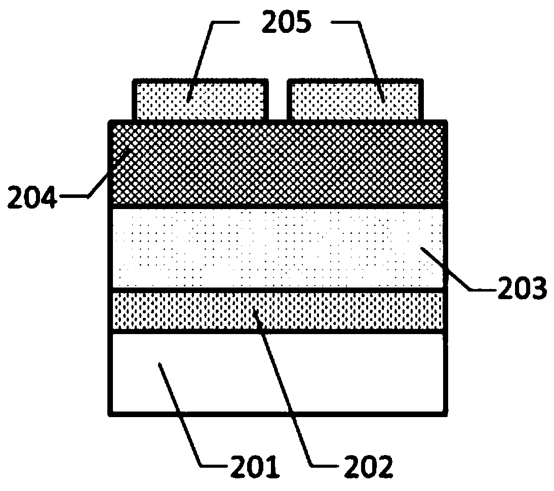
[0031] figure 2 It is a schematic structural diagram of a resistive memory device prepared based on InP resistive memory material, specifically: substrate material 201, the substrate material is single crystal silicon, and there is a silicon...

Embodiment 1

[0033] The preparation method and application of InP resistive memory materials, specifically including:

[0034] 1) The preparation method of the InP resistive memory material, the preparation steps are as follows: the InP target is fixed on the target holder of the PLD cavity, and then the Si / SiO with Pt / Ti electrodes deposited on the surface 2 Put the substrate into the sample holder in the cavity of the pulsed laser equipment, adjust the distance between the target substrates to 7cm, and then use the molecular pump to vacuum the cavity of the PLD equipment to 5×10 -8 Pa, use an electric furnace wire to heat the sample holder to 400°C, use a KrF excimer laser with a wavelength of 248nm as the laser source, set the laser parameters as follows: pulse frequency 5Hz, single pulse energy 240mJ, energy density 1.8J / cm 2 , and then start the laser to start depositing the InP resistive memory material on the substrate. The deposition time is 20 minutes, and the thickness of the InP...


PUM

PropertyMeasurementUnit
thicknessaaaaaaaaaa
thicknessaaaaaaaaaa
thicknessaaaaaaaaaa

Abstract

The invention discloses a preparation method and application of an InP resistive storage material, belonging to the technical field of microelectronics manufacturing. The preparation method comprises the following steps: 1) loading a single crystal InP sheet as a target into a cavity of a pulsed laser device; 2) loading a substrate with electrodes deposited on its surface into a cavity of a pulsed laser device; 3) placing a substrate in a pulsed laser device 4) Heating the substrate; 5) Depositing an InP film on the substrate by pulsed laser deposition; 6) Annealing the substrate deposited with the InP film at 600-800°C under vacuum conditions, and obtaining InP after cooling. Resistive storage materials. The InP resistive memory material has good storage characteristics, and the resistive memory prepared based on this memory material has the characteristics of wide storage window, long data retention time and high durability.

Description

technical field [0001] The invention belongs to the technical field of microelectronics manufacturing, and in particular relates to a preparation method and application of an InP resistive storage material. Background technique [0002] With the vigorous development of portable consumer electronic products, people put forward higher and higher requirements on the capacity and integration density of non-volatile memory. In order to increase the integration density of memory, the size of devices has been continuously reduced, multi-value storage technology has been widely used, and 3D stacking technology has gradually become a research hotspot. However, the reduction of device size will eventually reach the physical limit, and there are many problems in the reliability and other performance of multi-valued storage technology, while 3D technology faces many difficult challenges such as material selection, device structure, and process realization difficulty. It will not be pro...

Claims


Application Information

Patent Timeline
Patent Type & Authority Patents(China)
IPC IPC(8): H01L45/00C23C14/34
CPCC23C14/34H10N70/881H10N70/041H10N70/011
Inventor 赵鸿滨屠海令魏峰杨志民张国成
Owner GRIMAT ENG INST CO LTD
Why Eureka
Try Eureka