
A preparation method of transparent conductive oxide film-nanowire network

An oxide thin film, transparent and conductive technology, applied in the field of optoelectronic technology and new energy materials, can solve the problems of many oxygen defects in nanowires, difficult to control the length of the region where nanowires grow, and unable to independently control the position and size of catalysts. The effect of high resource utilization

Active Publication Date: 2019-07-09
HEFEI INSTITUTES OF PHYSICAL SCIENCE - CHINESE ACAD OF SCI
View PDF5 Cites 0 Cited by
  • Summary
  • Abstract
  • Description
  • Claims
  • Application Information

AI Technical Summary

Problems solved by technology

Although in a special ITO system, In-Sn alloy can be used as a catalyst to self-catalyze the growth of ITO nanowires, and since the gaseous In-Sn source acts as both the source of nanowire growth and the catalyst particles, it can be used in a single growth Branched ITO nanowire structures were observed, such as by electron beam evaporation [Journal of AppliedPhysics, 83(1995)1998], molecular beam epitaxy [Nature Nanotechnology 4(2009) 239], pulsed laser deposition [Materials Letters66(2012) 280 ] methods have obtained bifurcated ITO nanowires, but self-catalysis growth has the following disadvantages: First, self-catalysis cannot independently control the position and size of the catalyst, so it is not easy to control the growth area of ​​the nanowires (the entire substrate will be growth) and the length of the main and bifurcated nanowires (in parallel); secondly, in order to ensure that the In-Sn liquid alloy can continuously guide the growth of the nanowires, the growth of the ITO nanowires needs to be at a lower oxygen partial pressure (to prevent In-Sn Oxidation into a solid state), there are many oxygen defects in nanowires; third, self-catalysis is only applied in a few systems, and other transparent conductive oxides FTO and ATO cannot be applied

Method used


Image

  • A preparation method of transparent conductive oxide film-nanowire network
  • A preparation method of transparent conductive oxide film-nanowire network
  • A preparation method of transparent conductive oxide film-nanowire network

Examples


Embodiment 1

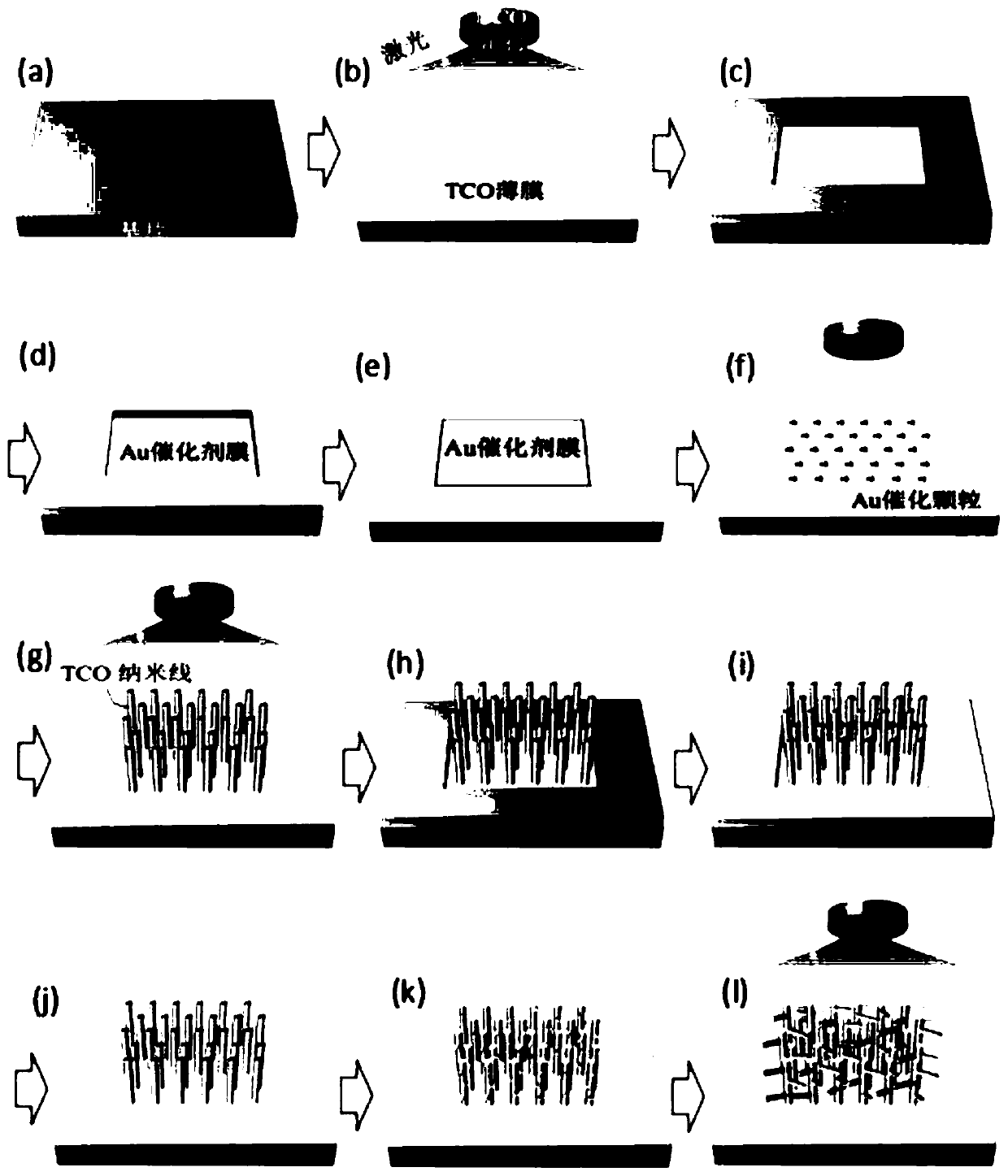
[0037] Step 1, transparent conductive oxide film growth:

[0038] The transparent substrate (material: ordinary glass) is ultrasonically cleaned with acetone, isopropanol, and deionized water in sequence, and after drying with nitrogen, it is treated with ultraviolet and ozone (150W ultraviolet lamp, treated in air for 10 minutes);

[0039] Place the cleaned substrate into the pulsed laser deposition chamber at 10 -3 Under the oxygen atmosphere of Pa, the substrate was heated to 100°C, the energy of the krypton fluoride excimer laser was controlled to be 20mJ, the repetition frequency was 2Hz, and the transparent conductive oxide target (FTO) was sputtered for 10min, and the surface of the substrate grew Transparent conductive oxide film, the thickness of the transparent conductive oxide film is 50nm;

[0040] Step 2, gold catalyst film deposition: take out the substrate with the transparent conductive oxide film deposited on the surface in step 1, and stick a metal mask on t...

Embodiment 2

[0044] Step 1, transparent conductive oxide film growth:

[0045] The transparent substrate (material: alumina single crystal) is ultrasonically cleaned with acetone, isopropanol, and deionized water in sequence, and after drying with nitrogen, it is treated with ultraviolet and ozone (150W ultraviolet lamp, treated in air for 10 minutes);

[0046] Place the cleaned substrate into the pulsed laser deposition chamber at 10 -1 Under the oxygen atmosphere of Pa, the substrate was heated to 350°C, the energy of the krypton fluoride excimer laser was controlled to be 60mJ, the repetition frequency was 10Hz, and the transparent conductive oxide target (ITO) was sputtered for 60min, and the surface of the substrate grew Transparent conductive oxide film, the thickness of the transparent conductive oxide film is 400nm;

[0047] Step 2, gold catalyst film deposition: take out the substrate with the transparent conductive oxide film deposited on the surface in step 1, and stick a metal...

Embodiment 3

[0051] Step 1, transparent conductive oxide film growth:

[0052] The transparent substrate (material: quartz glass) is ultrasonically cleaned with acetone, isopropanol, and deionized water in sequence, and after drying with nitrogen, it is treated with ultraviolet and ozone (150W ultraviolet lamp, treated in air for 10 minutes);

[0053] Place the cleaned substrate into the pulsed laser deposition chamber at 10 -2 Under the oxygen atmosphere of Pa, the substrate was heated to 300°C, the energy of the krypton fluoride excimer laser was controlled to be 40mJ, the repetition frequency was 10Hz, and the transparent conductive oxide target (FTO) was sputtered for 30min, and the surface of the substrate grew Transparent conductive oxide film, the thickness of the transparent conductive oxide film is 300nm;

[0054] Step 2, gold catalyst film deposition: take out the substrate with the transparent conductive oxide film deposited on the surface in step 1, and stick a metal mask on t...


PUM

PropertyMeasurementUnit
thicknessaaaaaaaaaa
thicknessaaaaaaaaaa
diameteraaaaaaaaaa

Abstract

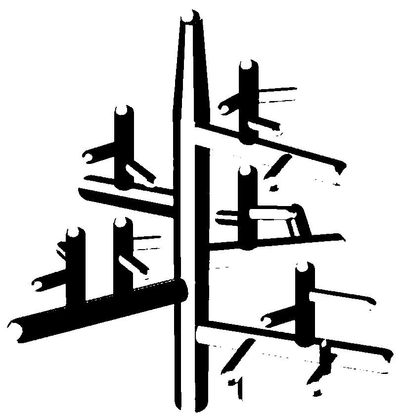
The invention relates to a preparation method of a transparent conductive oxide film-nanowire network. The method comprises the steps of (1) growing a transparent conductive oxide film on the surfaceof a clean substrate by using a pulse laser deposition method; (2) taking out the substrate with the transparent conductive oxide film deposited on the surface and depositing a gold catalyst film in aspecified area on the surface of the transparent conductive oxide film; and (3) growing transparent conductive nanowires on the surface of the gold catalyst film by using the pulse laser deposition method. A multistage branching nanowire network is obtained through repeating the steps (2) and (3). The invention provides a method for designing an artificial nanowire network in the micro-nano scale. According to the preparation method, growth of multiple transparent conductive oxide nanowires, including indium tin oxide and fluorine and antimony-doped tin oxide, in the specified area of the transparent conductive substrate can be achieved, and self-assembled growth, including branching growth in each step, of the nanowires can be finely adjusted.

Description

technical field [0001] The invention belongs to the field of photoelectric technology and new energy materials, and in particular relates to a method for preparing a transparent conductive oxide film-nanowire network. Background technique [0002] Transparent conductive oxides (TCO), represented by indium tin oxide (ITO), fluorine-doped tin oxide (FTO) and antimony-doped tin oxide (ATO), have both visible light transmittance, electrical conductivity and good Thermal and chemical stability, in the field of optoelectronics such as transparent display, touch screen, light-emitting diodes, construction fields such as smart windows, energy conversion fields such as solar photovoltaic devices, photolysis of water to produce hydrogen, and lithium / sodium ion batteries, supercapacitors and other energy There are important applications in the field of storage. The cost-effective advantages of transparent conductive oxide thin films have also promoted the rapid development of related ...

Claims


Application Information

Patent Timeline
Patent Type & Authority Patents(China)
IPC IPC(8): H01B13/00H01B1/08C23C14/34
CPCC23C14/3485H01B1/08H01B13/00
Inventor 孟钢方晓东陶汝华董伟伟王时茂
Owner HEFEI INSTITUTES OF PHYSICAL SCIENCE - CHINESE ACAD OF SCI
Learn More