SrFeOx resistive random access memory with multi-valued characteristic as well as preparation and application of SrFeOx resistive random access memory

A resistive memory and characteristic technology, applied in the field of semiconductor information storage, can solve problems such as limiting the storage capacity of devices, and achieve the effect of increasing storage capacity

Active Publication Date: 2022-04-15
HUAZHONG UNIV OF SCI & TECH +1
View PDF11 Cites 0 Cited by
  • Summary
  • Abstract
  • Description
  • Claims
  • Application Information

AI Technical Summary

Problems solved by technology

The above two types of SrFeO x RRAM can only form two states of high resistance state (High Resistance State, HRS) and low resistance state (Low Resistance State, LRS), which limits the storage capacity of the device per unit area

Method used


Image

  • SrFeOx resistive random access memory with multi-valued characteristic as well as preparation and application of SrFeOx resistive random access memory
  • SrFeOx resistive random access memory with multi-valued characteristic as well as preparation and application of SrFeOx resistive random access memory
  • SrFeOx resistive random access memory with multi-valued characteristic as well as preparation and application of SrFeOx resistive random access memory

Examples


preparation example Construction

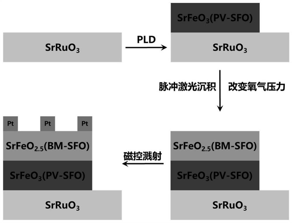
[0040] The present invention also provides the preparation method of the resistive memory device, comprising the following steps:

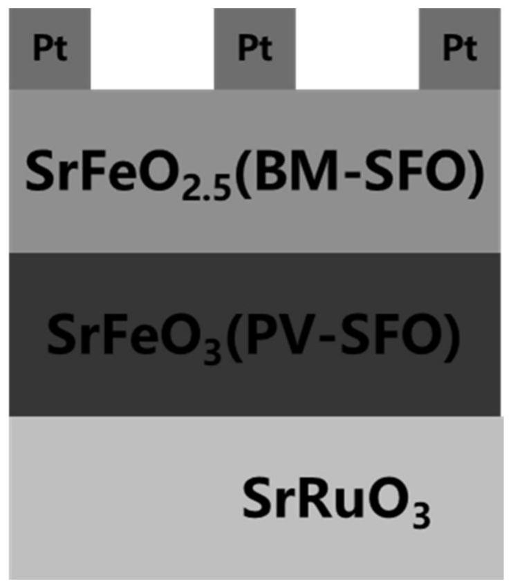
[0041] (1) The lower electrode and the first variable resistance layer SrFeO are sequentially deposited on the cleaned substrate using a pulsed laser deposition process. m Thin films, where 2.7≤m≤3;

[0042] (2) Using a pulsed laser deposition process on the first variable resistance layer SrFeO m Deposition of the second variable resistance layer SrFeO on the surface of the film 2.5 film;

[0043] (3) Magnetron sputtering and photolithography are used in the second resistance change layer SrFeO 2.5 The top electrode is prepared by deposition on the surface of the thin film.

[0044] In some embodiments, the process conditions of the pulsed laser deposition in step (1): the temperature is 650-700°C, the cavity atmosphere is oxygen, the air pressure is 3-10Pa, the laser energy is 250-450mJ, and the laser frequency is 1-8Hz , the vacuum degree ...

Embodiment 1

[0048] (1) Ultrasonic cleaning of SrTiO in acetone, ethanol, deionized water 3 15 minutes for each substrate;

[0049] (2) Use pulsed laser deposition to prepare SrRuO on the substrate described in step (1) 3 For the lower electrode, the process conditions are as follows: temperature is 680°C, chamber atmosphere is oxygen, air pressure is 10Pa, laser energy is 250mJ, laser frequency is 4Hz, vacuum degree is 5×10 -6 Pa, the distance between substrate and target is 55mm; SrRuO 3 The film thickness is 50 nm.

[0050] (3) Prepare SrFeO on the lower electrode described in step (2) using pulsed laser deposition 3 Thin film, the process conditions are: temperature is 650°C, chamber atmosphere is oxygen, air pressure is 5Pa, laser energy is 250mJ, laser frequency is 4Hz, vacuum degree is 5×10 -6 Pa, the distance between the lower electrode and the target is 55mm; SrFeO 3 The film thickness is 40 nm.

[0051] (4) SrFeO after completion of step (3) 3 Preparation of SrFeO by chang...

Embodiment 2

[0054] (1) Ultrasonic cleaning of SrTiO in acetone, ethanol, deionized water 3 15 minutes for each substrate;

[0055] (2) Use pulsed laser deposition to prepare SrRuO on the substrate described in step (1) 3 For the lower electrode, the process conditions are as follows: temperature is 680°C, chamber atmosphere is oxygen, air pressure is 10Pa, laser energy is 250mJ, laser frequency is 4Hz, vacuum degree is 5×10 -6 Pa, the distance between substrate and target is 55mm; SrRuO 3 The film thickness is 50 nm.

[0056] (3) Prepare SrFeO on the lower electrode described in step (2) using pulsed laser deposition 3 Thin film, the process conditions are: temperature is 650°C, chamber atmosphere is oxygen, air pressure is 5Pa, laser energy is 250mJ, laser frequency is 4Hz, vacuum degree is 5×10 -6 Pa, the distance between the lower electrode and the target is 55mm, SrFeO 3 The film thickness is 50nm;

[0057] (4) SrFeO after completion of step (3) 3 Preparation of SrFeO by changi...


PUM

PropertyMeasurementUnit
thicknessaaaaaaaaaa
thicknessaaaaaaaaaa
thicknessaaaaaaaaaa

Abstract

The invention belongs to the technical field of semiconductor information storage, and more particularly relates to a SrFeOx resistive random access memory with a multi-valued characteristic, and preparation and application of the SrFeOx resistive random access memory. The resistive random access memory sequentially comprises a substrate, a lower electrode, a first resistance change layer, a second resistance change layer and a top electrode from bottom to top, the first resistance change layer and the second resistance change layer are made of SrFeOm and SrFeO2.5, m is larger than or equal to 2.7 and smaller than or equal to 3, and the first resistance change layer provides a required oxygen ion source for the second resistance change layer to form conductive wires and interface diffusion. The SrFeOx resistive random access memory can have four stably existing resistance states through the structural design, and the technical problem that the storage capacity of the device under unit area is limited due to the fact that the device of the SrFeOx RRAM in the prior art can only form two states of high configuration and low resistance at present is solved.

Description

technical field [0001] The invention belongs to the technical field of semiconductor information storage, and more specifically, relates to SrFeO with multi-valued characteristics x Resistive memory, its preparation and application. Background technique [0002] With the rapid development of information technology today, the industry's demand for data processing and storage is increasing exponentially. With the popularization of 5G communication technology, data generated by consumer terminal electronic products, big data storage centers, and advanced research fields such as artificial intelligence Volume doubles every two years. As of 2020, the global data volume has reached 44 Zettabytes. In order to cope with the huge burden of data growth, it is urgent to iteratively upgrade the existing storage architecture. As the main force for storing data, the current mainstream development direction of flash memory NAND Flash is to increase the storage capacity per unit area by s...

Claims


Application Information

Patent Timeline
Patent Type & Authority Applications(China)
IPC IPC(8): H01L45/00C23C14/08C23C14/28C23C14/35
CPCC23C14/28C23C14/35C23C14/08H10N70/883H10N70/026
Inventor 程伟明苏睿陈家宝缪向水
Owner HUAZHONG UNIV OF SCI & TECH
Why Eureka
Try Eureka