Epitaxial structure and preparation method of deep ultraviolet multi-quantum well semiconductor laser
A multi-quantum well and epitaxial structure technology, which is applied in the field of epitaxial structure growth and preparation of deep ultraviolet multi-quantum well semiconductor lasers, can solve the problems of unfavorable product progress and development, large laser volume and high cost, and achieve high photoelectric conversion efficiency , high growth quality and precise component control
- Summary
- Abstract
- Description
- Claims
- Application Information
AI Technical Summary
Problems solved by technology
Method used
Image
Examples
Embodiment 1
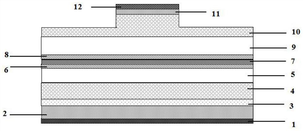
[0058] Epitaxial structure of deep ultraviolet multi-quantum well semiconductor laser: including a thickness of doping concentration 3E18cm -3 , an N-type single crystal substrate 2 with a thickness of 660 μm; an N-type transition layer 3 (thickness is 300 nm, Al x N y x / y=1-0.45 in the material, the value of x / y decreases with increasing thickness), N-type lower confinement layer 4 (thickness is 1.6 μm, Al x N y x / y=0.40 in the material), the lower waveguide layer 5 (thickness is 0.15μm, Al x N y x / y=0.55-0.7 in the material, and the x / y value increases with thickness), lower barrier layer 6 (thickness is 10nm, Al x N y x / y=0.85 in the material), multi-quantum well layer 7 (3 single quantum well layers, 2 barrier layers, a barrier layer is sandwiched between every two single quantum well layers, and the thickness of the single quantum well layer is 6.5nm, x / y=0.1, barrier layer thickness is 8nm, x / y=0.85), upper barrier layer 8 (thickness is 10nm, Al x N y x / y=0.85 in...
Embodiment 2
[0077] Epitaxial structure of deep ultraviolet multi-quantum well semiconductor laser: including a thickness of doping concentration 3E18cm -3 An N-type single crystal Si substrate 2 with a thickness of 640 μm; an N-type transition layer 3 (thickness is 500 nm, Al x N y x / y=1-0.40 in the material, the value of x / y gradually decreases with thickness), N-type lower confinement layer 4 (thickness is 2 μm, Al x N y x / y=0.40 in the material), the lower waveguide layer 5 (thickness is 0.25μm, Al x N y x / y=0.55-0.68 in the material, the x / y value increases uniformly with the thickness), the lower barrier layer 6 (thickness is 10nm, Al x N y x / y=0.83 in the material), multi-quantum well layer 7 (3 quantum well layers, thickness is 7nm, x / y=0.95, barrier layer is sandwiched between adjacent quantum well layers, barrier layer thickness is 8nm, x / y=0.85), upper barrier layer 8 (thickness is 10nm, Alx N y x / y=0.83 in the material), upper waveguide layer 9 (thickness is 0.25μm, Al ...
PUM
| Property | Measurement | Unit |
|---|---|---|
| thickness | aaaaa | aaaaa |
| thickness | aaaaa | aaaaa |
| thickness | aaaaa | aaaaa |
Abstract
Description
Claims
Application Information


