

Indium phosphide resistance variable material-based resistive random access memory and preparation method thereof
A technology of resistive variable memory and indium phosphide, which is applied in the direction of electrical components, etc., can solve the problems of rare research on resistive variable memory, and achieve the effect of improving defect state, good uniformity and stable optical performance
- Summary
- Abstract
- Description
- Claims
- Application Information
AI Technical Summary
Problems solved by technology
Method used
Image

Examples
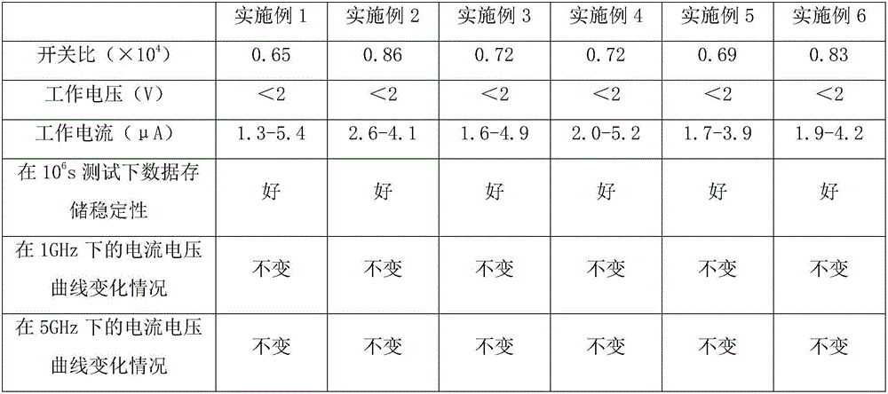
Embodiment 1
[0030] (1) In the high-pressure single crystal furnace, high-purity indium with a purity of 6N and high-purity red phosphorus with a purity of 6N are used as the main raw materials, indium sulfide and iron phosphide are used as dopants, and oxides with a water content of 500-2000ppm are used. Boron is used as a liquid sealant. Phosphorus-rich indium phosphide melts are obtained by using phosphorus injection rapid synthesis technology, and then seed crystals are introduced for crystal growth. Under an argon atmosphere, the crystals are pulled at a speed of 10mm / h to obtain a doped material with a diameter of 75mm. Single crystal indium phosphide sheets of S and Fe.
[0031] (2) Use the insulating inorganic material with platinum metal deposited on the surface as the substrate, put the single crystal indium phosphide sheet as the target into the cavity of the impact-resistant laser equipment, and put the insulating inorganic material substrate with electrodes deposited on the sur...
Embodiment 2
[0034] (1) In the high-pressure single crystal furnace, high-purity indium with a purity of 6N and high-purity red phosphorus with a purity of 6N are used as the main raw materials, indium sulfide and iron phosphide are used as dopants, and oxides with a water content of 500-2000ppm are used. Boron is used as a liquid sealant. Phosphorus-rich indium phosphide melts are obtained by using phosphorus injection rapid synthesis technology, and then seed crystals are introduced for crystal growth. Under an argon atmosphere, the crystals are pulled at a speed of 15mm / h to obtain a doped material with a diameter of 50mm. Single crystal indium phosphide sheets of S and Fe.
[0035] (2) Use the insulating inorganic material with platinum metal deposited on the surface as the substrate, put the single crystal indium phosphide sheet as the target into the cavity of the impact-resistant laser equipment, and put the insulating inorganic material substrate with electrodes deposited on the sur...
Embodiment 3
[0038] (1) In the high-pressure single crystal furnace, high-purity indium with a purity of 6N and high-purity red phosphorus with a purity of 6N are used as the main raw materials, indium sulfide and iron phosphide are used as dopants, and oxides with a water content of 500-2000ppm are used. Boron is used as a liquid sealant. Phosphorus-rich indium phosphide melts are obtained by using phosphorus injection rapid synthesis technology, and then seed crystals are introduced for crystal growth. Under an argon atmosphere, crystals are pulled at a speed of 12mm / h to obtain a doped indium phosphide with a diameter of 58.6mm. Single crystal indium phosphide sheet doped with S and Fe.
[0039](2) Use the insulating inorganic material with platinum metal deposited on the surface as the substrate, put the single crystal indium phosphide sheet as the target into the cavity of the impact-resistant laser equipment, and put the insulating inorganic material substrate with electrodes deposite...
PUM
| Property | Measurement | Unit |
|---|---|---|
| thickness | aaaaa | aaaaa |
| thickness | aaaaa | aaaaa |
| diameter | aaaaa | aaaaa |
Abstract
Description
Claims
Application Information