Unpowered micro-flow control chip for heavy metal ion on site detection and making and using method thereof
A technology of microfluidic chips and heavy metal ions, which is applied in chemical method analysis, measuring devices, biological testing, etc., can solve problems such as difficult to implement on-site detection applications, temperature changes, etc., and achieve low cost and simple operation
- Summary
- Abstract
- Description
- Claims
- Application Information
AI Technical Summary
Problems solved by technology
Method used
Image

Examples
Embodiment 1
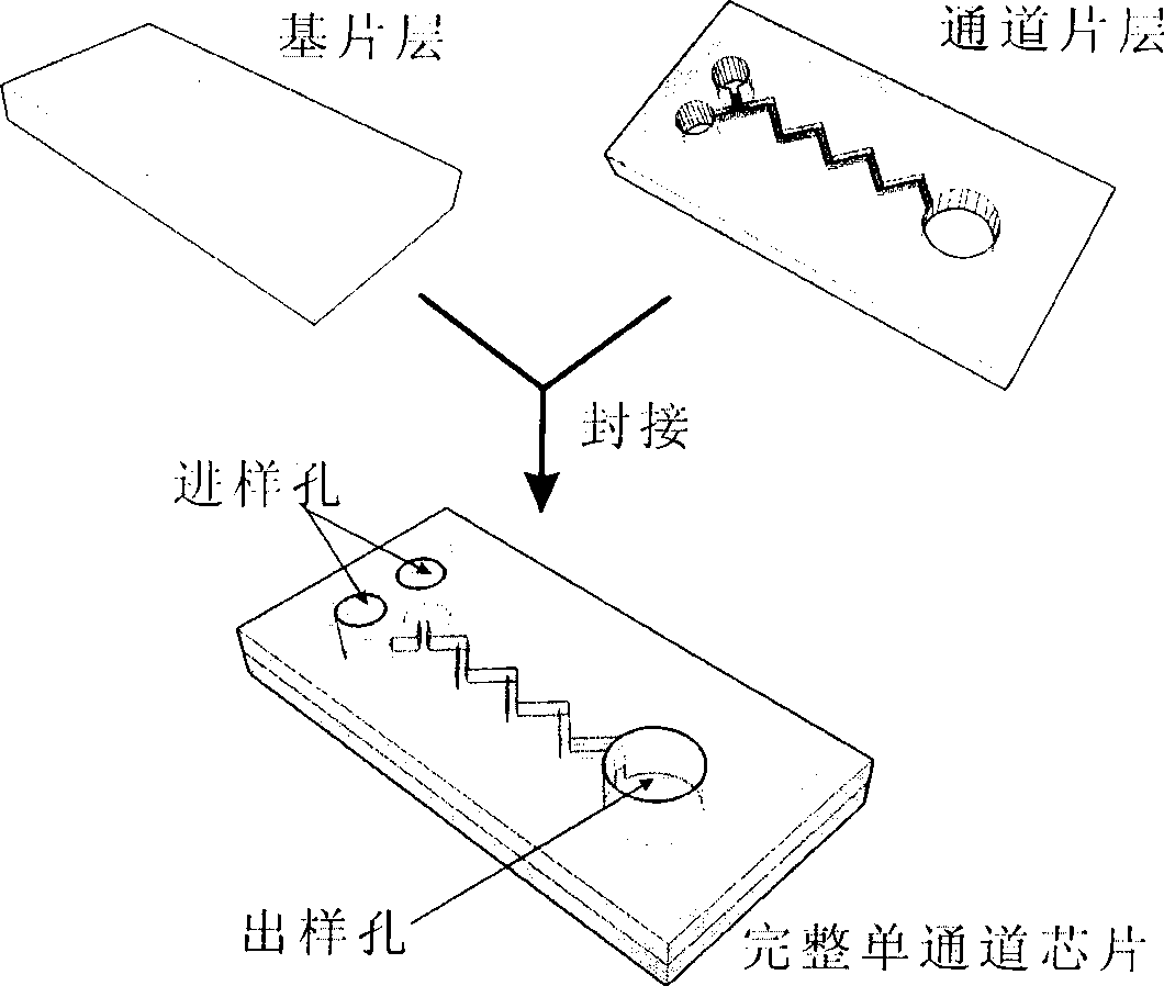
[0040] 1. Using a silicon wafer distributed with photoetched patterns as a positive mold, using polydimethylsiloxane (PDMS) as a substrate, and using conventional methods in the field, fabricate 8 microfluidic channels (channel width 100 microns, with a depth of 20 microns) of PDMS channel sheets. After the PDMS channel sheet is peeled off from the mould, a puncher is used to punch holes at the end mark of the microchannel as a sample inlet (2mm in diameter) and a sample outlet (3mm in diameter), and its specific size is adjustable. And the glass petri dish is used as a mold, and the substrate layer is made of PDMS.
[0041] 2. Seal the PDMS channel layer and the substrate layer, put it in a glass drying dish and pump it with a vacuum pump for one hour, and immediately seal the end of the sample hole with tape after taking it out, and leave it for about 3-5 minutes. (If spare, seal and place in a sealed bag)
[0042] 3. Nanogold probes functionalized with poly-T nucleotide c...
Embodiment 2
[0060] 1. Using a silicon wafer distributed with photoetched patterns as a positive mold, using polydimethylsiloxane (PDMS) as a substrate, and using conventional methods in the field, fabricate 8 microfluidic channels (channel width 100 Micron, thickness of 3mm) PDMS channel sheet. After the PDMS channel sheet is peeled off from the mould, a puncher is used to punch holes at the end mark of the microchannel as a sample inlet (2mm in diameter) and a sample outlet (3mm in diameter), and its specific size is adjustable. And the glass petri dish is used as a mold, and the substrate layer is made of PDMS.
[0061] 2. Seal the PDMS channel layer and the substrate layer, put it in a glass drying dish and pump it with a vacuum pump for one hour, and immediately seal the end of the sample hole with tape after taking it out, and leave it for about 3-5 minutes. (If spare, seal and place in a sealed bag)
[0062] 3. Add the assembled nano-gold probes functionalized with mercaptoundecan...
PUM
| Property | Measurement | Unit |
|---|---|---|
| Thickness | aaaaa | aaaaa |
| Thickness | aaaaa | aaaaa |
| Thickness | aaaaa | aaaaa |
Abstract
Description
Claims
Application Information
 - Generate Ideas
- Intellectual Property
- Life Sciences
- Materials
- Tech Scout
- Unparalleled Data Quality
- Higher Quality Content
- 60% Fewer Hallucinations
Browse by: Latest US Patents, China's latest patents, Technical Efficacy Thesaurus, Application Domain, Technology Topic, Popular Technical Reports.
© 2025 PatSnap. All rights reserved.Legal|Privacy policy|Modern Slavery Act Transparency Statement|Sitemap|About US| Contact US: help@patsnap.com