

Method for forming and etching hard mask layer
A hard mask layer, technology to be etched, applied in the direction of electrical components, semiconductor/solid-state device manufacturing, circuits, etc. Effect
- Summary
- Abstract
- Description
- Claims
- Application Information
AI Technical Summary
Problems solved by technology
Method used
Image

Examples
no. 1 example
[0056] This embodiment introduces a new method for forming a hard mask layer, Figure 5 is a flow chart of the method for forming a hard mask layer according to the first embodiment of the present invention, Figure 6 to Figure 7 In order to illustrate the device cross-sectional view of the first embodiment of the present invention, below in conjunction with Figure 5 to Figure 7 A first embodiment of the present invention will be described in detail.
[0057] Step 501: Provide a substrate.
[0058] The substrate may be a substrate on which a metal oxide semiconductor transistor has been formed, or a substrate on which an underlying metal wiring structure has been formed. Usually its surface already has a layer to be etched.
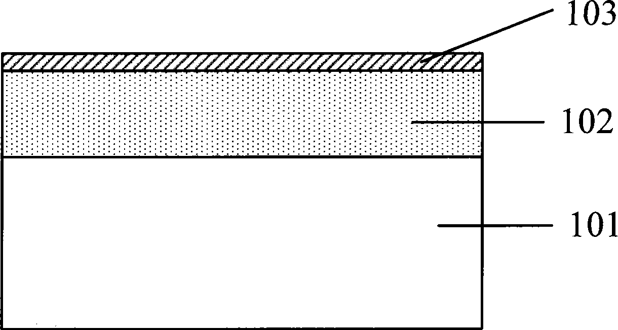
[0059] Step 502: forming an initial hard mask layer on the substrate.
[0060] Image 6 It is a schematic cross-sectional view of the device after forming the initial hard mask layer in the first embodiment of the present invention, as Image 6 As ...
no. 2 example
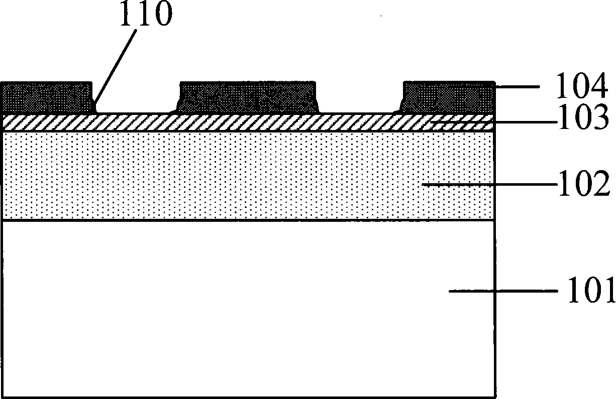
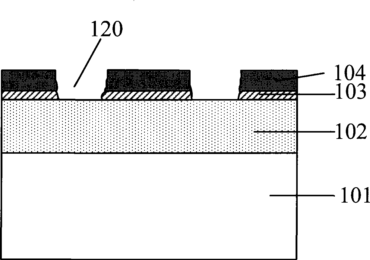
[0082] This embodiment introduces an etching method using a hard mask layer, Figure 8 It is a flowchart of the etching method of the second embodiment of the present invention, Figure 9 to Figure 14 In order to illustrate the cross-sectional view of the device of the second embodiment of the present invention, below in conjunction with Figure 8 to Figure 14 A second embodiment of the present invention will be described in detail.
[0083] Step 801: providing a substrate, and a layer to be etched has been formed on the substrate.
[0084] The substrate may be a substrate on which a metal oxide semiconductor transistor has been formed, or a substrate on which an underlying metal wiring structure has been formed.
[0085] The etching method in this embodiment uses a hard mask layer to assist the photoresist to protect and define the etched pattern. Before forming the hard mask layer, usually a layer to be etched is formed on its surface, and the layer to be etched in this e...
PUM
 Abstract
Description
Claims
Application Information