Supercharge Your Innovation With Domain-Expert AI Agents!

VCSEL array device and manufacturing method thereof

A technology of devices and diode arrays, which is applied in the field of surface light-emitting semiconductor array devices, can solve problems such as internal stress faults, and achieve the effect of suppressing the increase of dislocations

Active Publication Date: 2012-10-31
FUJIFILM BUSINESS INNOVATION CORP
View PDF3 Cites 0 Cited by
  • Summary
  • Abstract
  • Description
  • Claims
  • Application Information

AI Technical Summary

Problems solved by technology

However, further studies have found that not only dislocations occur due to oxidation, but also the internal stress between the oxidized region and the interlayer insulating film formed near the oxidized region is also the cause of sudden failure

Method used


Image

  • VCSEL array device and manufacturing method thereof
  • VCSEL array device and manufacturing method thereof
  • VCSEL array device and manufacturing method thereof

Examples


Embodiment Construction

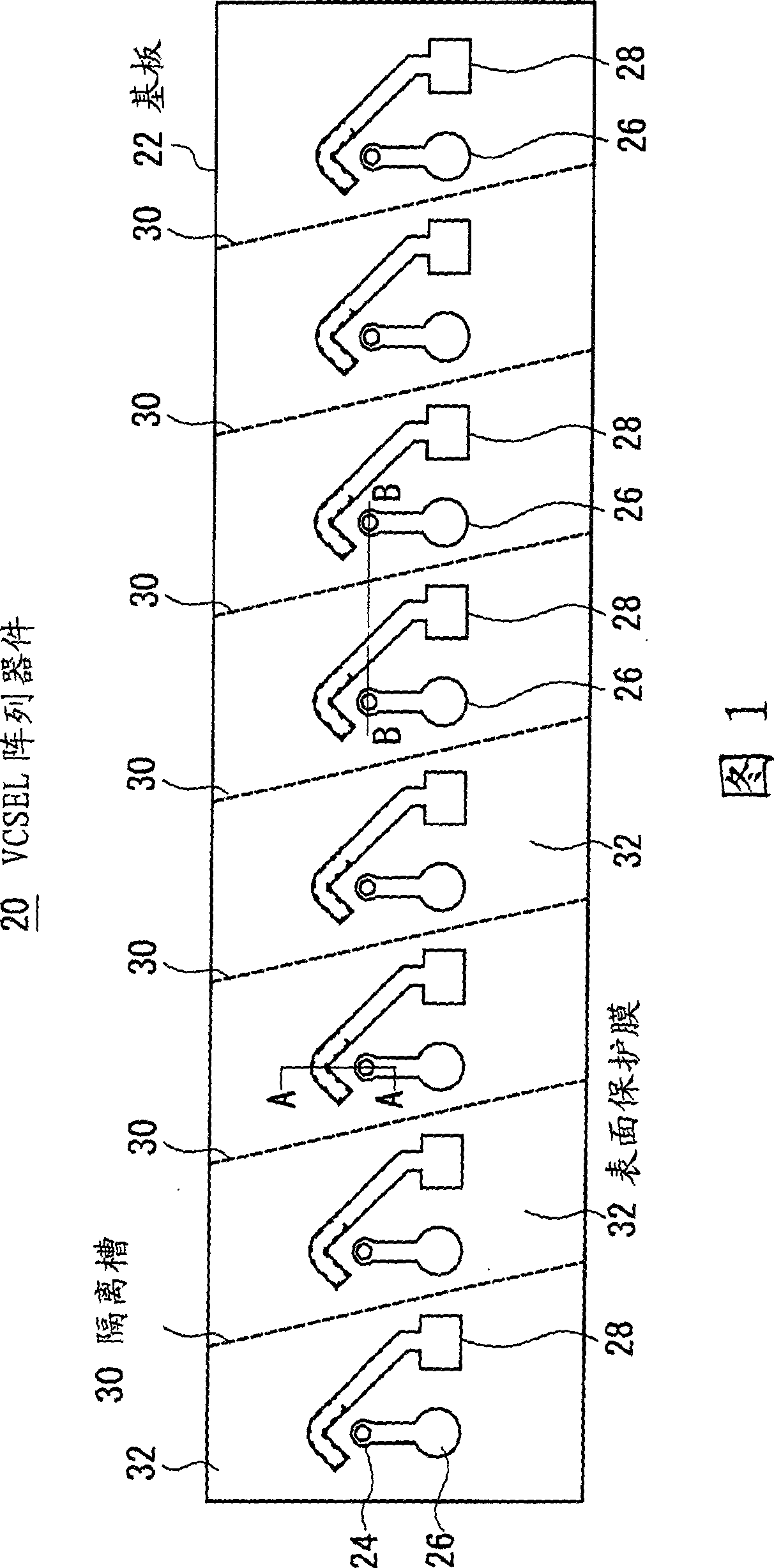
[0033]Embodiments of the selective oxidation VCSEL array device according to aspects of the present invention will be described below with reference to the accompanying drawings.

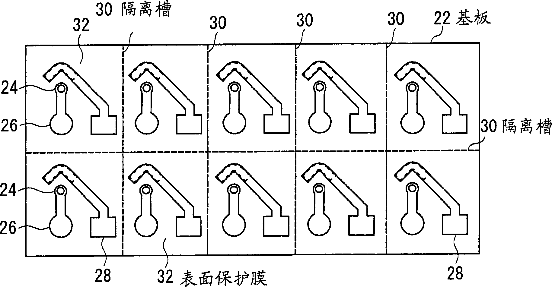
[0034] figure 1 is a schematic plan view of a selective oxidation VCSEL array device according to an embodiment of the present invention. exist figure 1 In the illustrated array device 20 , a plurality of mesa portions 24 (light emitting portions) are linearly arranged on a rectangular substrate 22 . On the substrate, eight mesa portions 24 can be formed at approximately constant intervals. On the substrate, a plurality of p-side electrodes 26 and a plurality of n-side electrodes 28 may be formed corresponding to the mesa portion 24 . The p-side electrode 26 is electrically connected to the p-type contact layer on top of the mesa portion 24 . The n-side electrode 28 is electrically connected to the n-type semiconductor layer of the mesa portion 24 . When a forward bias current is applied to t...


PUM


Abstract

Provided is a VCSEL array device (20) that includes at least a first multilayer reflective film, an active layer, and a second multilayer reflective film, formed on a substrate (22) that extends in a longitudinal direction. Plural mesa portions (24) are formed on the substrate by selectively removing at least a portion of the first multilayer reflective film, active layer, and second multilayer reflective film. A selectively oxidized region is formed in at least one of the first multilayer reflective film and the second multilayer reflective film. The VCSEL array device further includes an interlayer insulating film that covers at least a side portion and a bottom portion of the mesa portions, and a surface protecting film (32) that covers the interlayer insulating film. The surface protecting film (32) has plural grooves (30) formed along a longitudinal direction of the substrate in which at least a portion of the surface protecting film is removed.

Description

technical field [0001] The present invention relates to a surface emitting semiconductor array device, and more particularly to a stacked layered structure of a vertical cavity surface emitting laser diode (hereinafter referred to as VCSEL) array device. The present invention also relates to a method of manufacturing such a VCSEL array device. Background technique [0002] VCSEL devices are a class of laser diodes that emit light from the surface of a semiconductor substrate. VCSELs have excellent properties that edge-emitting laser diodes do not have. For example, driving of VCSELs requires a lower current value (lower threshold current), and a characteristic test (non-destructive evaluation) can be performed when VCSELs are on a wafer, and VCSELs can be easily arranged in a two-dimensional array. Due to these characteristics, VCSELs have been used as light sources for optical data processors or optical communication devices, or data storage devices using light. [0003]...

Claims


Application Information

Patent Timeline
Patent Type & Authority Patents(China)
IPC IPC(8): H01S5/183
Inventor 松下和征植木伸明
Owner FUJIFILM BUSINESS INNOVATION CORP
Features
  • R&D
  • Intellectual Property
  • Life Sciences
  • Materials
  • Tech Scout
  • Unparalleled Data Quality
  • Higher Quality Content
  • 60% Fewer Hallucinations
Learn More