

Silicon crystallization method
A silicon crystallization and crystallization technology, applied in chemical instruments and methods, crystal growth, single crystal growth and other directions, can solve the problems of polysilicon film film quality reduction and low heat treatment temperature, and achieve the effect of improving various characteristics and film quality.
- Summary
- Abstract
- Description
- Claims
- Application Information
AI Technical Summary
Problems solved by technology
Method used
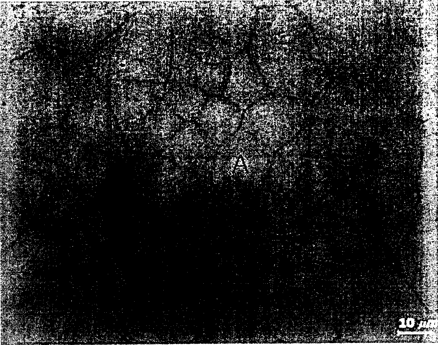
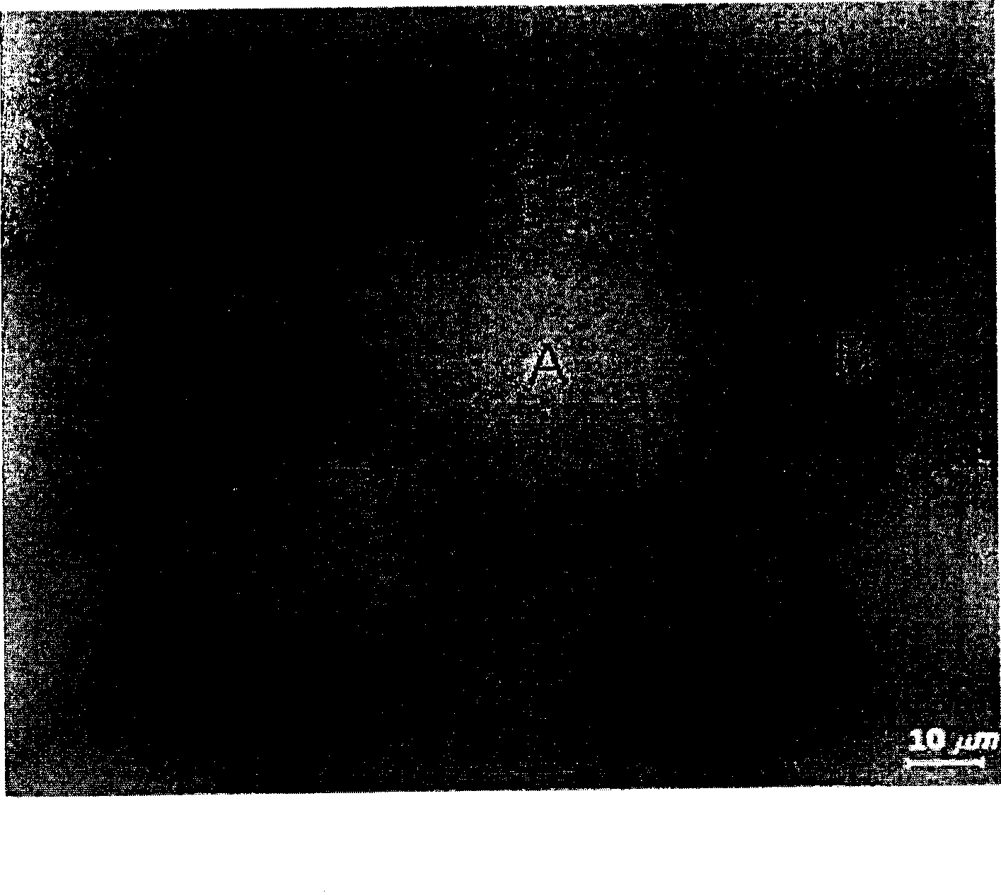
Image

Examples
Embodiment Construction
[0032] The inventors of the present invention recognized the problem in the silicon crystallization method using the above-mentioned conventional low-temperature crystallization method, and conducted diligent research to solve the problem. In the induced crystallization method, nuclei (nucleation) of silicon crystal grains are generated at the first heat treatment temperature, and after they are grown to complete crystallization, further heat treatment is performed at a temperature higher than the first heat treatment temperature (second heat treatment temperature), Accordingly, polycrystalline silicon having an excellent film quality for removing defects existing in grown silicon crystal grains was produced, thereby completing the present invention. Therefore, the present invention is characterized in that silicon is crystallized by a two-step heat treatment process after introducing a metal catalyst onto amorphous silicon.
[0033] The method for crystallizing silicon accord...
PUM
 Abstract
Description
Claims
Application Information