BCD semiconductor device and manufacturing method thereof

A semiconductor and device technology, applied in the field of semiconductor power devices, can solve the problem of high cost and achieve the effects of excellent performance, low manufacturing cost and low output impedance

Inactive Publication Date: 2009-06-10
UNIV OF ELECTRONIC SCI & TECH OF CHINA +1
View PDF0 Cites 33 Cited by
  • Summary
  • Abstract
  • Description
  • Claims
  • Application Information

AI Technical Summary

Problems solved by technology

However, the traditional manufacturing method

Method used


Image

  • BCD semiconductor device and manufacturing method thereof

Examples


Embodiment Construction

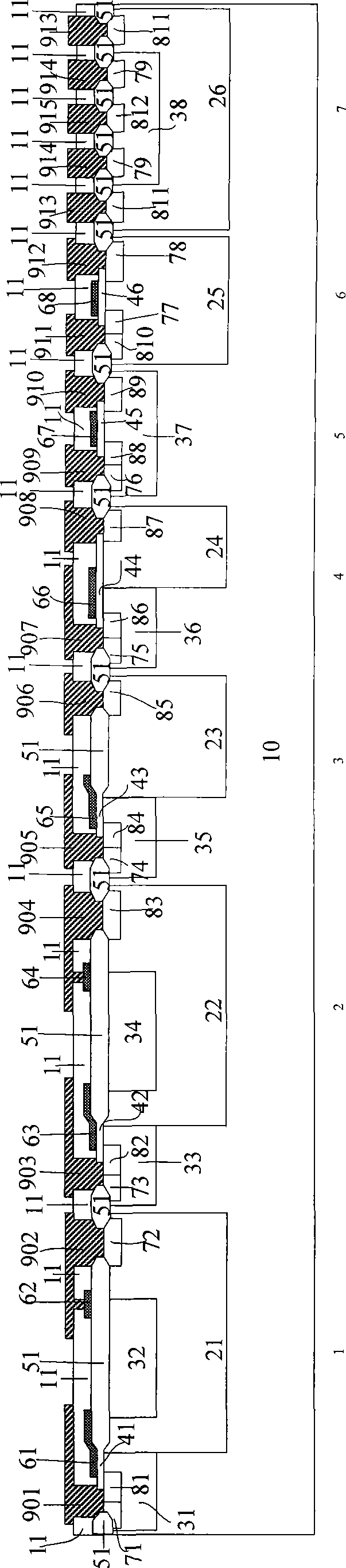
[0024] Referring to the accompanying drawings, it can be seen that the present invention provides a group of BCD semiconductor devices, which are directly fabricated on a single crystal substrate.

[0025]The high-voltage nLIGBT device 1 is directly made in the p-type substrate 10, 21 is the n-type drift region well of nLIGBT, 31 is the p-type body region of nLIGBT, 32 is the p-type falling field layer of nLIGBT, and 81 is the nLIGBT nLIGBT + Cathode area, 71 is the p of nLIGBT + Well contact area, 72 is the p of nLIGBT + Anode region, 51 is the field oxide layer of nLIGBT, 41 is the gate oxide layer of nLIGBT, 11 is the metal front dielectric of nLIGBT, 61 is the polysilicon gate of nLIGBT, 62 is the polysilicon field plate of nLIGBT, 901 is the cathode metal of nLIGBT, 902 It is the anode metal of nLIGBT. The p-type drop field layer 32 is located under the field oxide layer 51 and surrounded by the n-type drift region well 21, the p-type + The anode region 72 is under the...


PUM

PropertyMeasurementUnit
Thicknessaaaaaaaaaa

Abstract

The invention provides a BCD semiconductor device and a method for producing the same, and belongs to the technical field of a semiconductor power device. The device comprises a high-voltage nLIGBT, a first-class high-voltage nLDMOS, a second-class high-voltage nLDMOS, a third-class high-voltage nLDMOS, a low-voltage NMOS, a low-voltage PMOS and a low-voltage NPN. The semiconductor device is directly arranged on a single crystal substrate. The high-voltage nLIGBT, the high-voltage nLDMOSes and the low-voltage NPN are directly arranged on a single crystal p-type substrate, the low-voltage NMOS is arranged in a p-type well, and the low-voltage PMOS is arranged in an n-type well. During the production, the epitaxial process is not required. Single chips of the nLIGBT, the NLDMOSes, the low-voltage NMOS, the low-voltage PMOS and the low-voltage NPN are successfully integrated on the single crystal substrate. Because the epitaxial process is not required, the chips are relatively low in production cost. The nLIGBT device and nLDMOS devices of the invention have the characteristics of high input impedance, low output impedance and the like, and a high-voltage power integrated circuit formed by the nLIGBT device and the nLDMOS devices can be applied to various products in fields of electric consumption, display drive and the like.

Description

technical field [0001] The invention belongs to the technical field of semiconductor power devices. Background technique [0002] The development of high-voltage power integrated circuits is inseparable from high-voltage and low-voltage semiconductor devices. High-voltage power integrated circuits often use the high analog precision of Bipolar transistors, the high integration of CMOS, and the high power or voltage characteristics of DMOS (Double-diffused MOSFET) to integrate Bipolar analog circuits, CMOS logic circuits, CMOS analog circuits and DMOS high-voltage power devices. Monolithic integration. Lateral high-voltage DMOS (Lateral Double-diffused MOSFET, LDMOS) devices are widely used in high-voltage power integrated circuits because the drain, gate, and source are all on the chip surface, and are easy to integrate with low-voltage signal circuits through internal connections. However, the traditional manufacturing method requires the use of epitaxial technology, and ...

Claims


Application Information

Patent Timeline
IPC IPC(8): H01L27/06H01L21/8249
Inventor 乔明蒋苓利段双亮陈波赵磊张波
Owner UNIV OF ELECTRONIC SCI & TECH OF CHINA
Why Eureka
Try Eureka