Encapsulation structure and method for white light emitting diode device

A technology of light-emitting diodes and packaging structures, applied in semiconductor devices, electrical components, circuits, etc., can solve problems such as accelerating device failure

Inactive Publication Date: 2009-06-10
GUANGDONG REAL FAITH OPTO
View PDF0 Cites 54 Cited by
  • Summary
  • Abstract
  • Description
  • Claims
  • Application Information

AI Technical Summary

Problems solved by technology

These residual surface defects and impurities will further expand during potting a...

Method used


Image

  • Encapsulation structure and method for white light emitting diode device
  • Encapsulation structure and method for white light emitting diode device
  • Encapsulation structure and method for white light emitting diode device

Examples


Embodiment 1

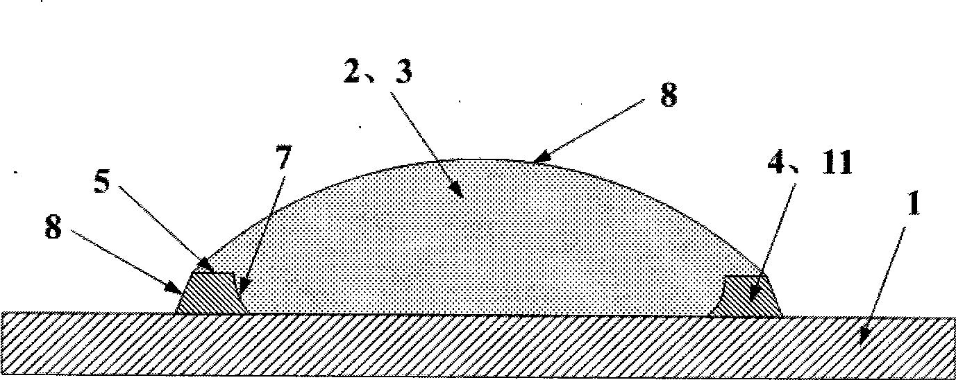
[0023] Embodiments of the present invention are further described below in conjunction with the accompanying drawings: see image 3 , the packaging structure of the white light emitting diode device is composed of a light emitting diode chip 10 , a packaging tube shell 1 , a packaging silica gel 2 , and a fluorescent powder glue 3 . The light emitting diode chip 9 is mounted in the packaging tube 1 . The packaging package 1 is in the shape of a flat plate or a structure with a reflective cup, which is flat in this embodiment. The structure of the packaging package 1 includes one or several packaging cells 4 , and a plurality of packaging cells 4 are included in this embodiment. The packaging unit 4 is a ring-shaped convex strip-shaped packaging unit 11 or a groove-shaped packaging unit 12 centered on the chip 10. The shape of the ring is a square or a circle or a regular polygon. Each packaging unit 4 can be Located on the same plane or on different planes, the multiple enca...

Embodiment 2

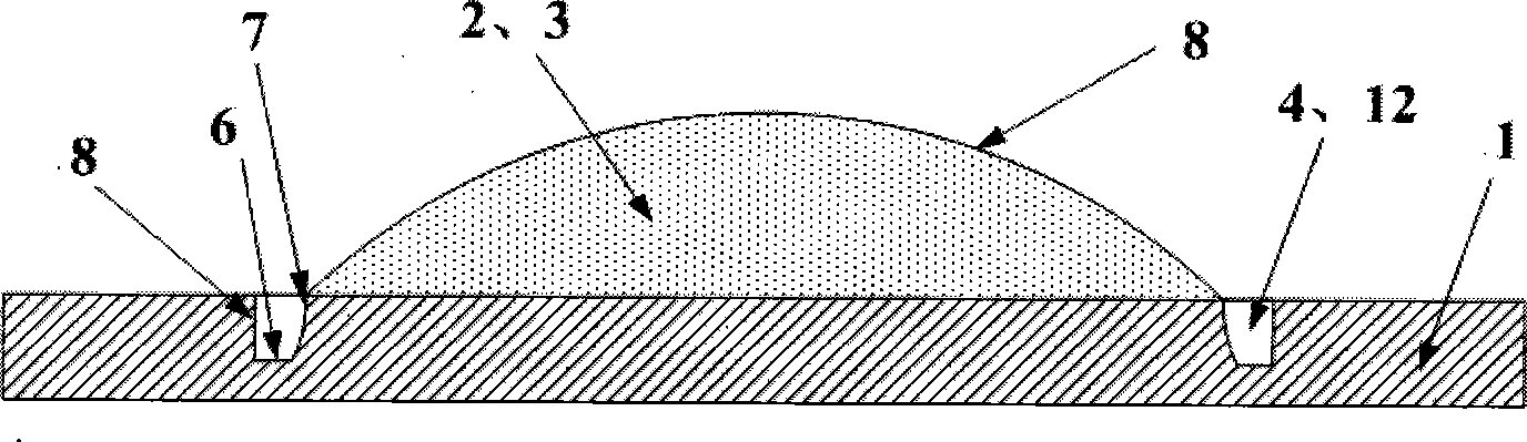
[0035] The difference between the second embodiment and the first embodiment is that the encapsulation unit 4 is a groove-shaped encapsulation unit 12, and the light-emitting diode chip 10 is first covered by the encapsulation silica gel 2, and then by the fluorescent powder glue 3, and the groove-shaped encapsulation The monomer 12 is made by precision cutting or mold manufacturing or stamping manufacturing or laser manufacturing. The outer surface 8 of each groove-shaped packaging unit 12 is a vertical plane in this embodiment, and the inner surface 7 is an arc surface in this embodiment, see Figure 4 .

Embodiment 3

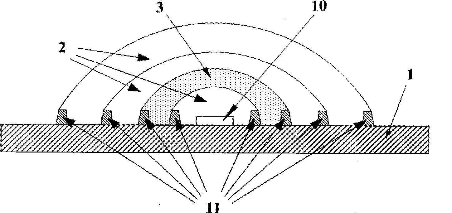
[0037]The difference between the third embodiment and the first embodiment is that the package package 1 has a reflector 13, and the package package 1 contains both a convex strip-shaped package unit 11 and a groove-shaped package unit 12, see Figure 5 .


PUM


Abstract

The invention provides a structure and a method for packaging white-light LED devices. The structure mainly comprises an LED chip, a packaging tube shell, packaging silica gel and phosphor gel. The structure is characterized in that the LED chip is pasted in the packaging tube shell; the LED chip is covered and packaged in the packaging tube shell by the packaging silica gel and the phosphor gel; the packaging silica gel is in a lens shape; the packaging tube shell consists of a plurality of packaging single-bodies; the periphery of each packaging single-body is provided with a convex strip or a groove; and the packaging silica gel and a phosphor layer are made into a monolayer or multilayer packaging body through the structural shape of the packaging single-bodies. The invention has the advantages of utilizing the own surface tension of the silica gel and the phosphor layer, limiting the own flowing of the silica gel and the phosphor layer through the structure on the packaging tube shell, forming the packaging body of a lens and the phosphor layer of which the surface shape meets design requirements, reducing cost and improving product quality.

Description

technical field [0001] The invention relates to a manufacturing method of a semiconductor device, in particular to a packaging structure and method of a white light emitting diode device. Background technique [0002] Light-emitting diode (LED) is an electroluminescent device processed by semiconductor manufacturing technology. Its light-emitting mechanism is to use the recombination of electrons and holes to generate photons. This recombination effect can theoretically approach 100% quantum efficiency under continuous current and stable voltage drive. This method of electric injection can also avoid large Stokes shift, so LED has the advantages of high luminous efficiency, good color rendering, low power consumption, energy saving and environmental protection, high safety and reliability, and long service life. [0003] Since the first blue LED chip was successfully developed, there are currently two main technologies for obtaining white LEDs. One is to use high-brightness...

Claims


Application Information

Patent Timeline
IPC IPC(8): H01L33/00H01L33/48H01L33/50
Inventor 刘胜刘宗源罗小兵王恺陈明祥甘志银金春晓
Owner GUANGDONG REAL FAITH OPTO
Why Eureka
Try Eureka