Low loss multilayered circuit board

A multi-layer circuit board and circuit technology, which is applied to printed circuit components, measuring electricity, measuring electrical variables, etc., to achieve the effect of making good use of circuit space

Inactive Publication Date: 2009-06-10
MICROELECTRONICS TECH INC
View PDF1 Cites 12 Cited by
  • Summary
  • Abstract
  • Description
  • Claims
  • Application Information

AI Technical Summary

Problems solved by technology

[0003] When laying out test circuit 10 on the multilayer printed circuit board 1 as shown in Figure 1, circuit 10 extends from the periphery to the inner ring and from top to bottom to pass through each laminated printed circuit board 100, on making, the circuit 10 The vertical transmission path is to drill through holes in each layer of circuit boards 100, and then arrange metal materials in the through holes to form high-conductivity guide holes 11. Holes 11 are used to arrange conductive metal sheets 12 of a specific width, and finally the layers of circuit boards 100 are stacked and pressed at high temperature to form transmission lines 10 extending in the multilayer circuit board 1, so that it can handle a large number of high-density circuits. Test transmission requirements; when applied to high-frequency transmission, the signal quality depends on the transmittable bandwidth and energy consumption. Once the high-frequency transmission line is laid inside the circuit board as in the above-mentioned multilayer printed circuit board 1, not only must be emphasized The length of the transmission line and the material of the interlayer circuit board are used to minimize the delay time of the signal response and the dielectric loss in the transmission process, and the vertical and horizontal layout of the transmission line in the circuit board needs to pay more attention to the matching of the characteristic impedance. In order to reduce the interface reflection loss caused by the discontinuity of the signal characteristic impedance as much as possible, the penetration loss of the high-frequency signal transmission in the entire multilayer circuit board 1 can be reduced without affecting the signal bandwidth. The line width will be extended after high-temperature lamination, so only a limited width and thickness can be used when laying the metal sheet 12 to take into account the utilization of circuit space. The characteristic impedance, on the contrary, causes the problem of impedance mismatch, and the high-frequency signal transmission line needs to be connected to the ground potential adjacent to the ground line to maintain the characteristic impedance required for high-frequency transmission. Therefore, if it is a low characteristic impedance The transmission line provides a high-speed response and low-loss high-frequency transmission environment. It is necessary to arrange a wider horizontal line on a single-layer circuit board and to arrange grounding lines in parallel with the surrounding horizontal and vertical space, so that the utilization of circuit space Efficiency is often unable to take into account a large number of high-intensity high-frequency test transmission requirements

Method used


Image

  • Low loss multilayered circuit board
  • Low loss multilayered circuit board
  • Low loss multilayered circuit board

Examples


Embodiment Construction

[0041] Hereinafter, several preferred embodiments are listed with reference to the accompanying drawings to describe the structure and functions of the present invention in detail.

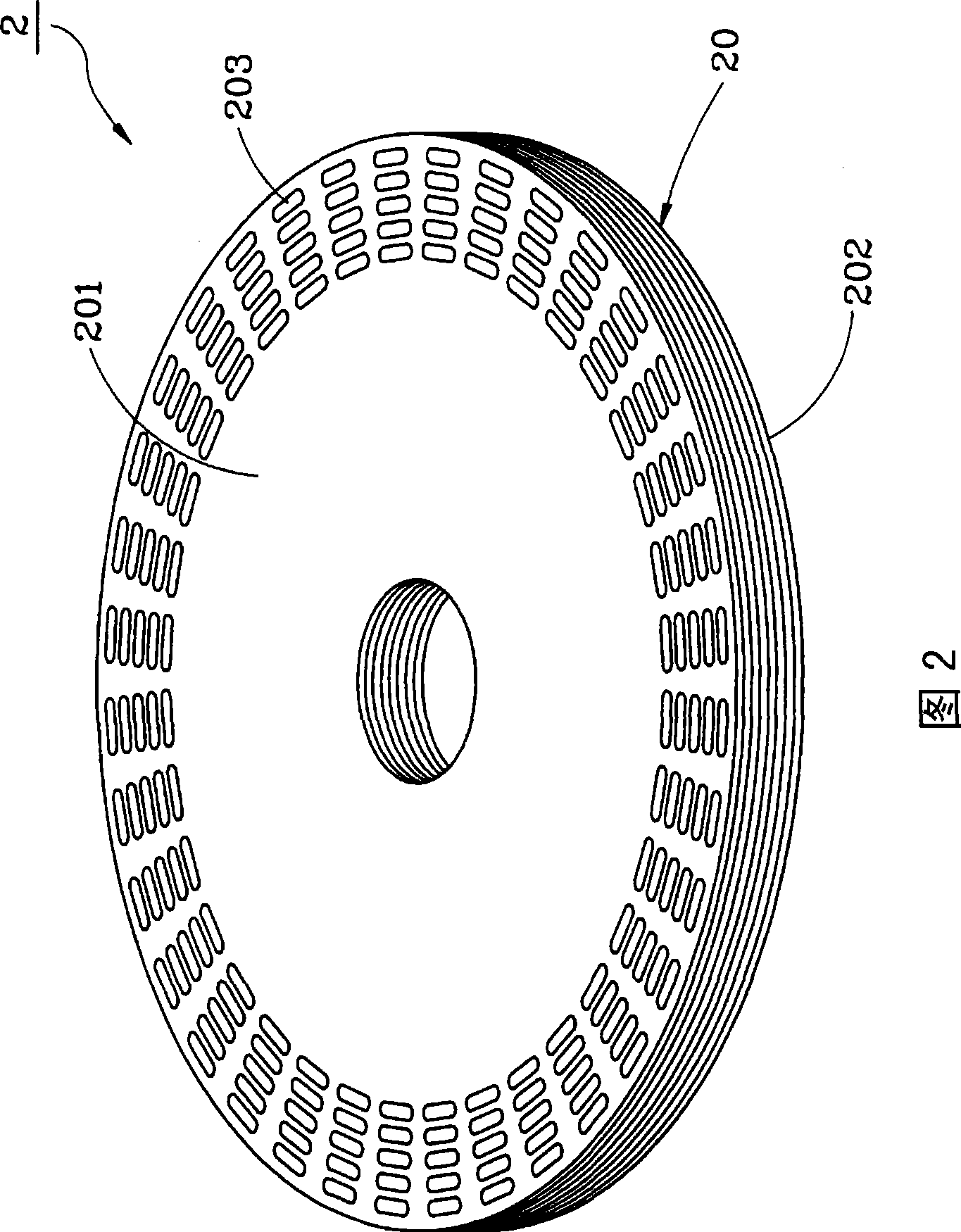
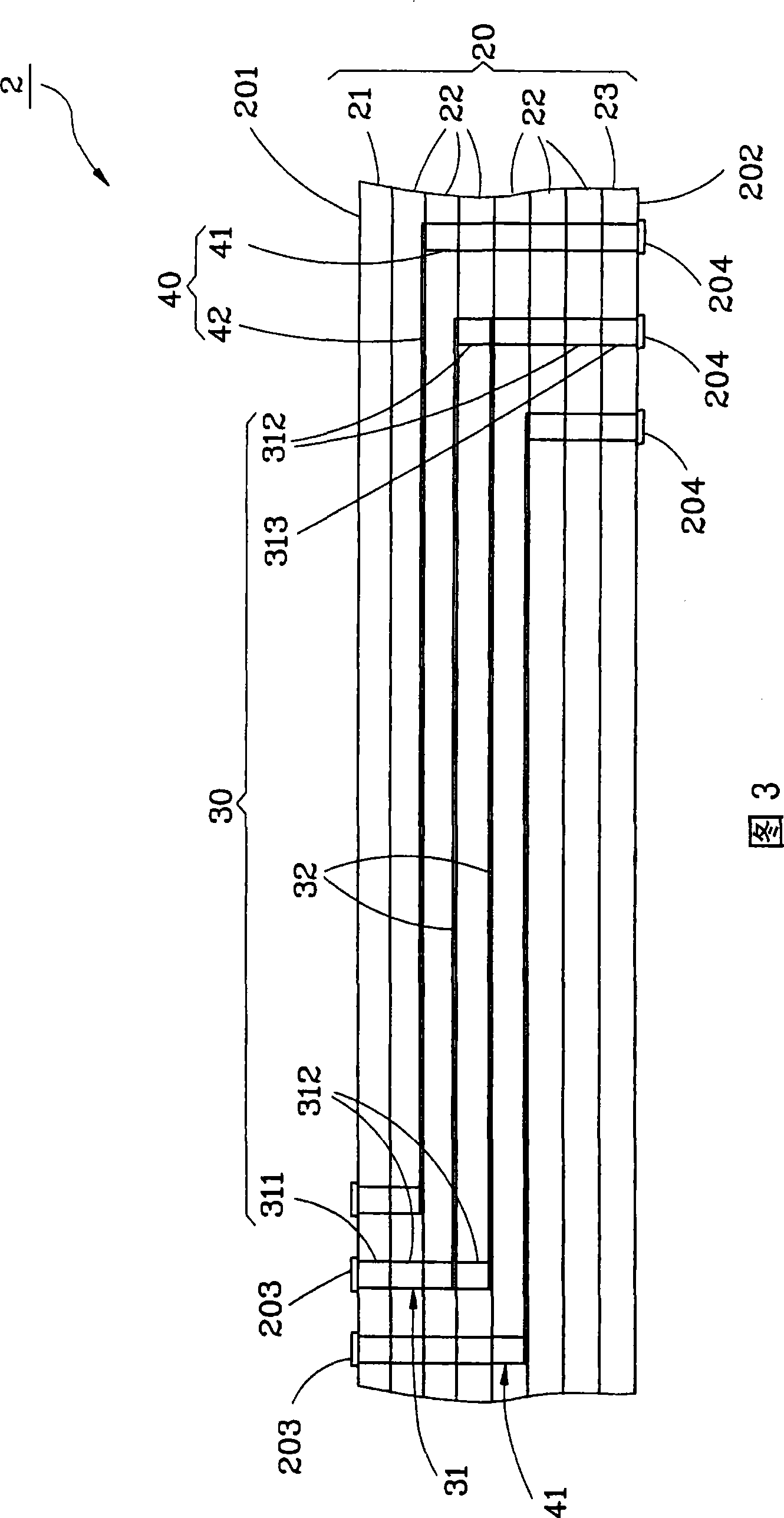
[0042] Please refer to Figure 2 to Figure 4 A multi-layer circuit board 2 provided by the most preferred embodiment of the present invention shown is a multi-layer printed circuit board of approximate integrated circuit wafer size, which is used on the wafer test probe card, and can be used for a wide range of The wafer circuit assembly is used for electrical testing, and a plurality of signal circuits 30 and grounding circuits 40 with high-frequency transmission line characteristics are laid out on a plurality of substrates 20 with good insulation properties, and then these substrates 20 are laminated and laminated. , the multilayer circuit board 2 has a relative upper and lower surfaces 201, 202, the upper surface 201 is provided with a plurality of upper solder joints 203 near the periphery, an...


PUM


Abstract

The present invention relates to a multi-layer circuit board, which comprises a plurality of substrates which are overlapped up and down and signal circuits and grounding circuits which are arranged on the substrates. Extending from an upper welding spot arranged on the uppermost substrate to a lower welding spot arranged on the lowermost substrate, each signal circuit is provided with at least two signal conducting wires which extend horizontally and the two signal conducting wires are adjacent up and down, in parallel and mutually shorted electrically. Each signal circuit is adjacently provided with the grounding circuits which extend with the signal circuits in parallel and are electrically connected to the grounding electric potential.

Description

technical field [0001] The invention relates to a multilayer circuit board, in particular to a multilayer printed circuit board with high-frequency circuits. Background technique [0002] In the probe card used for wafer-level testing, the pads on the upper side of the circuit board of the probe card are touched by the test head of the test machine, so that the transmission lines connected to the corresponding pads transmit the test signal of the test machine to the On the densely arranged probes near the center of the circuit board, when the corresponding electronic components of the wafers touched by each probe receive the test signal, the corresponding electrical characteristics are sent back to the test machine through the probe card for analysis , so in the whole wafer-level test process, the transmission line design of the probe card circuit board has a very important influence on the test results of electronic components, especially as electronic technology becomes mo...

Claims


Application Information

Patent Timeline
IPC IPC(8): H05K1/02G01R1/02
Inventor 顾伟正简志忠赖俊良黄千惠罗嘉和
Owner MICROELECTRONICS TECH INC
Why Eureka
Try Eureka