Method for preparing film GaN LED based on plane bonding and temporality substrate transfer technology

A temporary, substrate technology, applied in the direction of electrical components, circuits, semiconductor devices, etc., can solve problems such as cracks, poor bonding force of support components, uneven surface of GaN epitaxial film, etc., achieve high yield, reduce cracks, The effect of reducing the propagation of cracks

Active Publication Date: 2009-06-24
XIAMEN SANAN OPTOELECTRONICS TECH CO LTD
View PDF0 Cites 15 Cited by
  • Summary
  • Abstract
  • Description
  • Claims
  • Application Information

AI Technical Summary

Problems solved by technology

[0003] In order to solve the above-mentioned problem of poor bonding force with the supporting parts caused by the uneven surface of the GaN epitaxial film and the problem of cracks caused by the existence of gaps, in order to improve the yield of large-area laser lift-off removal of sapphire substrates, the present invention aims to propose a method based on planar Fabrication method of thin film GaN LED by bonding and temporary substrate transfer technology

Method used


Image

  • Method for preparing film GaN LED based on plane bonding and temporality substrate transfer technology
  • Method for preparing film GaN LED based on plane bonding and temporality substrate transfer technology
  • Method for preparing film GaN LED based on plane bonding and temporality substrate transfer technology

Examples


Embodiment Construction

[0021] The present invention will be further described below in conjunction with the accompanying drawings and embodiments.

[0022] Such as Figure 1a to Figure 1j A thin-film GaN LED preparation method based on planar bonding and temporary substrate transfer technology is shown, and its preparation steps are as follows:

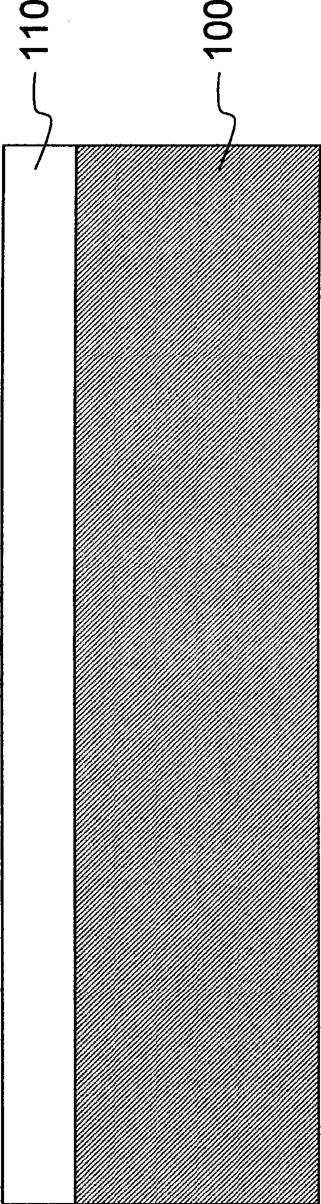
[0023] Step 1: If Figure 1a As shown, a GaN-based LED luminescent material 110 is epitaxially grown on a sapphire substrate 100 by metal-organic chemical vapor deposition (MOCVD);

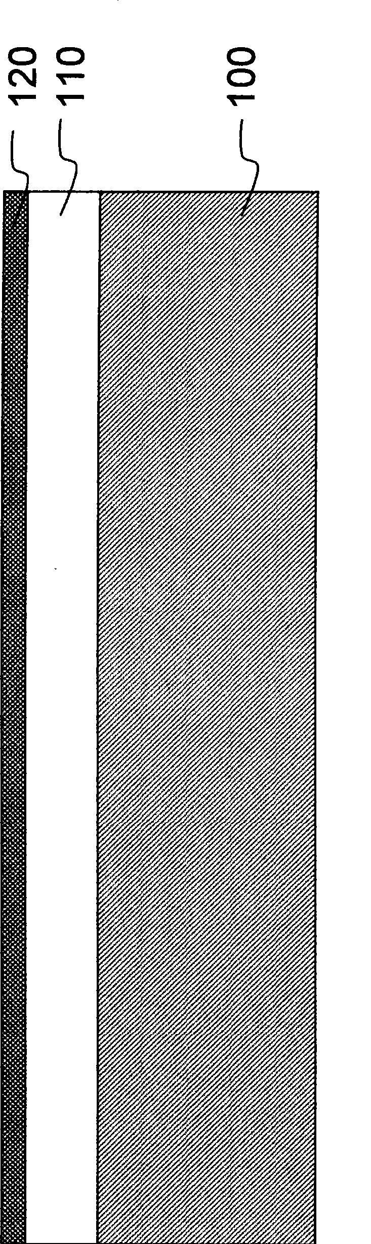
[0024] Step 2: If Figure 1b As shown, electron beam evaporation is used to deposit p metal and reflective metal film 120 on the surface of p-GaN. Ag is selected with a thickness of 100 nm. The ohmic contact and adhesion between metal film 120 and GaN-based semiconductor unit device 110 are improved by high temperature annealing. And form ohmic contact with p-GaN after high temperature annealing;

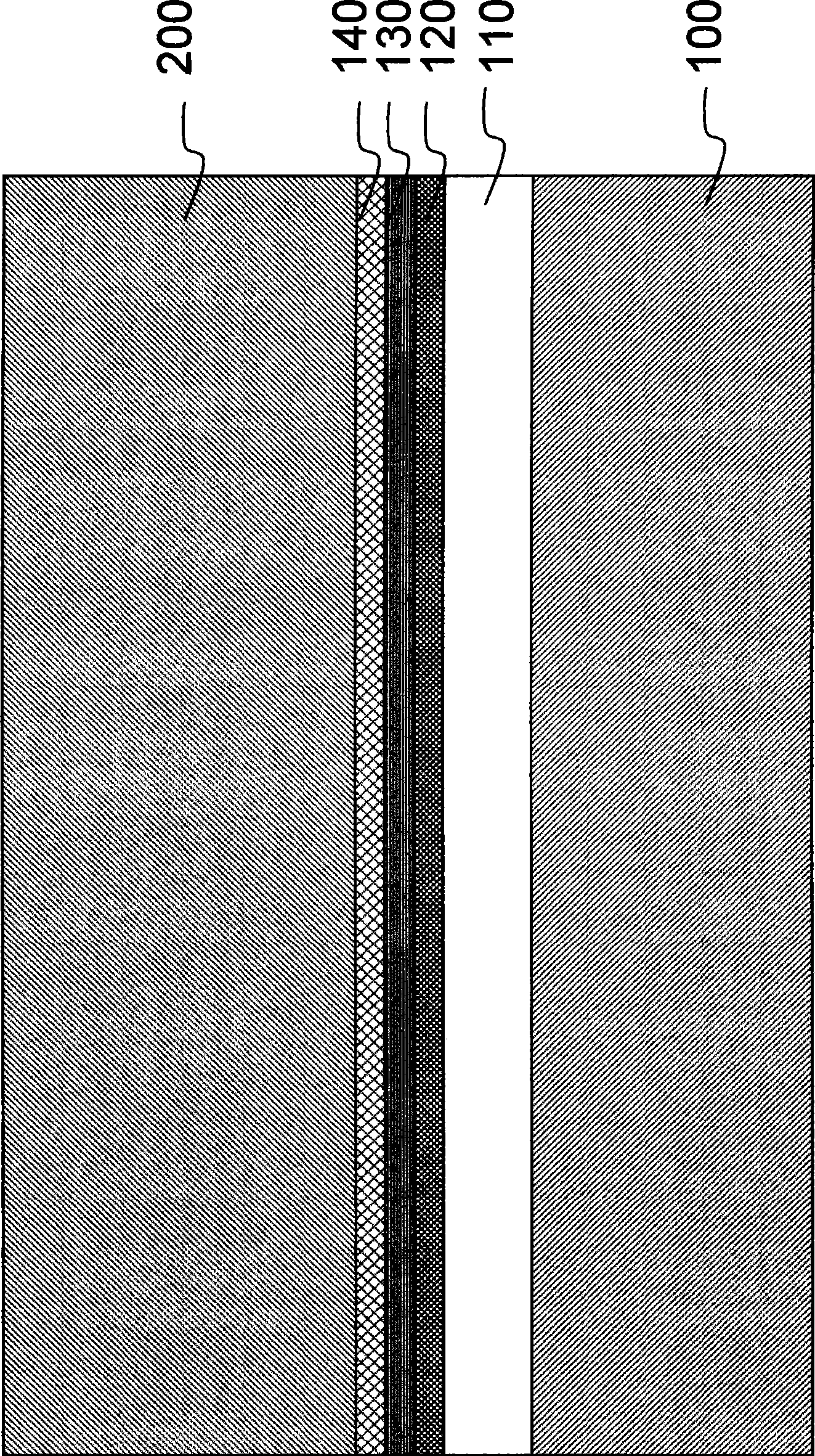
[0025] Step 3: If Figure 1c As shown, electron beam evaporation is used to ...


PUM


Abstract

The invention discloses a film GaN LED preparation method based on the plane bonding and temporary substrate transfer technology. In the method, a plane is firstly bonded on a support substrate and then unit devices are separated, so that the gapless seaming between the GaN LED and the support substrate can be realized; then the absolute separation among all the GaN LED devices is achieved so as to reduce the production and extension of the cracks in the laser stripping process; through the temporary substrate, chip manufacturing is carried out after the laser stripping to ensure high yield rate of GaN LED film production when the sapphire substrate is removed after large-area laser stripping.

Description

technical field [0001] The invention relates to a method for preparing a thin-film GaN light-emitting diode, in particular to a method for preparing a thin-film GaN LED based on planar bonding and temporary substrate transfer technology. Background technique [0002] At present, most GaN-based epitaxy is mainly grown on sapphire substrates. Due to the poor conductivity of sapphire, ordinary GaN-based light-emitting devices adopt a lateral structure, that is, the two electrodes are on the same side of the device, and the current flows laterally in the N-GaN layer. Flowing at unequal distances, there is current blockage and heat generation; in addition, the thermal conductivity of the sapphire substrate is low, thus limiting the luminous power and efficiency of GaN-based devices. Removing the sapphire substrate and making the light-emitting device into a vertical structure can effectively solve the problems of heat dissipation, light output and antistatic. At present, the meth...

Claims


Application Information

Patent Timeline
Patent Type & Authority Applications(China)
IPC IPC(8): H01L33/00
Inventor 林雪娇陈文欣洪灵愿潘群峰吴志强
Owner XIAMEN SANAN OPTOELECTRONICS TECH CO LTD
Why Eureka
Try Eureka