Apparatus and method for exploiting reverse short channel effects in transistor devices

A short-channel effect, transistor technology, applied in transistors, amplifiers with semiconductor devices/discharge tubes, semiconductor/solid-state device manufacturing, etc., can solve the problems of complex use of short-channel transistors, increase complexity, improve Linearity, effect of increasing circuit size

Inactive Publication Date: 2012-12-26
TELEFON AB LM ERICSSON (PUBL)
View PDF0 Cites 0 Cited by
  • Summary
  • Abstract
  • Description
  • Claims
  • Application Information

AI Technical Summary

Problems solved by technology

[0009] The use of short-channel transistors is further complicated by the so-called "reverse short-channel effect" (RSCE)

Method used


Image

  • Apparatus and method for exploiting reverse short channel effects in transistor devices
  • Apparatus and method for exploiting reverse short channel effects in transistor devices
  • Apparatus and method for exploiting reverse short channel effects in transistor devices

Examples


Embodiment Construction

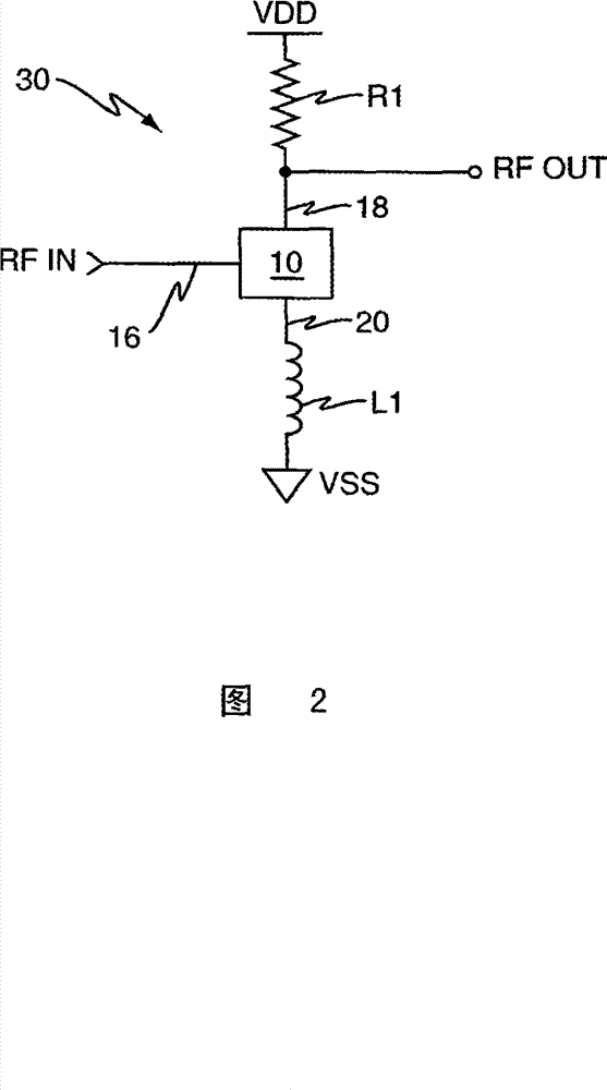
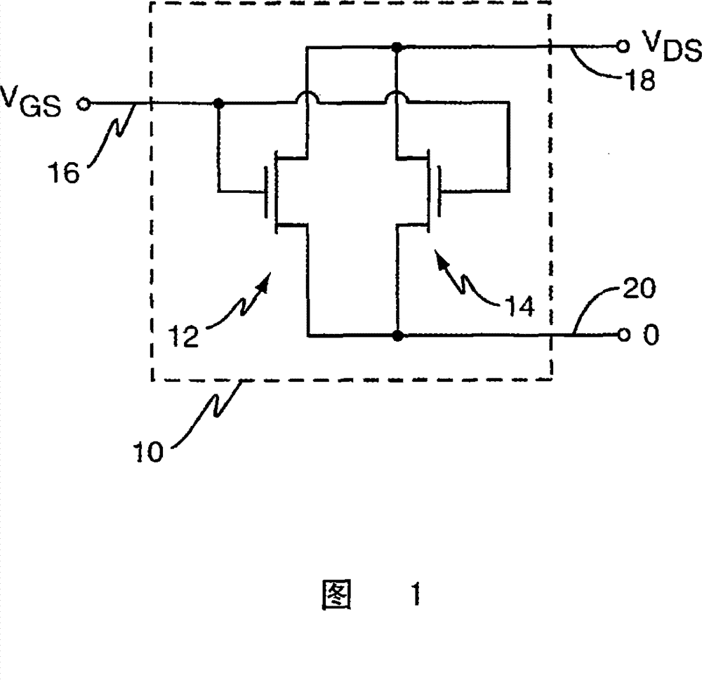
[0023] figure 1 A "composite" transistor circuit 10 is shown formed by coupling a first transistor 10 with a second transistor 14 in parallel such that the two transistors 12 and 14 share a gate connection 16 , a drain connection 18 and a source connection 20 . (For a bipolar embodiment of the transistor circuit 10, these connections correspond to base, collector and emitter connections, respectively). Noting that in one or more embodiments, the transistor circuit 10 is implemented in an integrated circuit process, wherein the first transistor 12 comprises two or more integrated circuit transistor elements configured to have a first transistor channel length, Instead, the second transistor 14 includes two or more integrated circuit transistor elements configured to have a second transistor channel length.

[0024] In one or more embodiments, the first and second transistors 12 and 14 have substantially the same threshold voltage curve as a function of transistor channel leng...


PUM


Abstract

A method of implementing a transistor circuit comprises coupling first and second transistors in parallel, wherein the first transistor has a channel length corresponding to a peak in the transistor's voltage threshold curve arising from reverse short channel effects, and the second transistor has a longer channel length and, therefore, a lower threshold voltage. Exploiting reverse short channel effects in this manner enables the implementation of "composite" transistor circuits that exhibit improved linearity.

Description

technical field [0001] The present invention relates generally to transistor devices, and more particularly to exploiting the reverse short channel effect in such devices. Background technique [0002] In most communication circuits, linear signal amplification represents a core enabling function. For example, wireless communication transceivers employ linear signal amplification at various stages in their transmit and receive signal processing paths. More particularly, radio frequency (RF) based communication systems rely on linear amplification in frequency mixing circuits, low noise amplification circuits, power amplification circuits, etc., to maintain signal fidelity and limit unwanted harmonic frequency generation. However, the non-linear current-voltage (IV) characteristics of semiconductor transistors, such as bipolar or MOS transistors, represent a fundamental source of signal non-linearity in communication circuits, which is heavily dependent on the use of these t...

Claims


Application Information

Patent Timeline
Patent Type & Authority Patents(China)
IPC IPC(8): H01L27/088
CPCH03F3/211H03F2200/492H01L27/088H03F2200/456H03F3/19H03F1/3205H03F2203/21178H01L21/823412H03F2200/451H03F3/45
Inventor T·亚伦伯
Owner TELEFON AB LM ERICSSON (PUBL)
Why Eureka
Try Eureka