Comparison device and analog-to-digital converter using the same
A comparison device and comparator technology, applied in the direction of analog/digital conversion calibration/test, analog/digital conversion, code conversion, etc., can solve the problem of slow time to reach the steady state operation state, achieve short stabilization time and smallest size Minimize and eliminate the effect of offset voltage
- Summary
- Abstract
- Description
- Claims
- Application Information
AI Technical Summary
Problems solved by technology
Method used
Image
Examples
Embodiment Construction
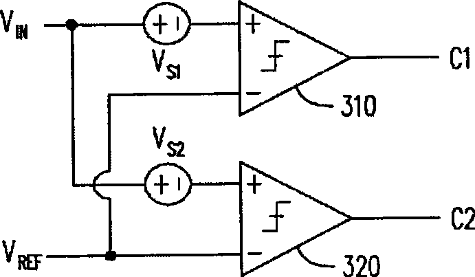
[0054] Figure 3A for an input signal with the same V IN and reference voltage V REF The circuit diagram of the two comparators. Figure 3B is a schematic diagram of the influence of the output signal of the comparator with offset voltage on the input signal. Please refer to Figure 3A and 3B , comparators 310 and 320 have different offset voltages V S1 and V S2 , that is to say the threshold voltage V of the comparator 310 T1 Equal to (V REF +V S1 ), and the threshold voltage of comparator 320 is equal to (V REF +V S2 ). Here it is assumed that the threshold voltage V T1 greater than the critical voltage V T2 . If the input signal V IN greater than (V REF +V S1 ), the output signal C1 of the comparator 310 has a logic high level (“1”), and the output signal C2 of the comparator 320 is also the same. If the input signal V IN less than (V REF +V S2 ), the output signal C1 of the comparator 310 has a logic low level (“−1”), and the output signal C2 of the co...
PUM
 Abstract
Description
Claims
Application Information


